論文リスト(Publication)
2026
International Conferences
- K. Ogura and K. Niitsu, “A 0.3 V Subthreshold CMOS Analog Front-End with Polyaniline pH Sensor for Biomedical Applications”, IEEE International Symposium on Olfaction and Electronic Nose (ISOEN 2026), May. 2026.
- S. Xu, K. Liu, L. Chan, H. Tagawa, H. Shinohara and K. Niitsu, “A Sub-Threshold All-nMOS Reconfigurable PUF with Secure Configuration Selection for Stable 6-Bits/Cell”, IEEE International Solid-State Circuits Conference (ISSCC 2026), Feb. 2026.
2025
Journals
- Y. Iwata, Y. Yanagizono, T. Iida, Y. Ashida, Y. Yamada, T. Asano, H. Suzuki, T. Tsuge, O. Komiyama and K. Niitsu, “Examination of the Communication Environment When Applying Removable Dentures as Wearable Devices”, Cureus Journal of Medical Science, Nov. 2025.
DOI: 10.7759/cureus.97531 - R. Zhang, Y. Cao, H. Zhang, Q. Cheng, S. Nishizawa, K. Niitsu and H. Shinohara, “Entropy Improvement in Latch-Based True Random Number Generator Using Negative Bias Temperature Instability”, IEEE Transactions on Circuits and Systems I, 2025.
DOI: 10.1109/TCSI.2025.3621604 - R. Sakai, K. Ishikawa, H. Kondo, K. Niitsu, M. Hiramatsu, H. Tanaka and M. Hori, “Platinum nanoparticle-decorated carbon nanowall anodes fabricated via top-down approach for abiotic glucose fuel cells”, Scientific Reports, Aug. 2025.
- H. Kitaike, H. Tagawa, S. Xu, R. Zhang, K. Liu, and K. Niitsu, “Design and Experimental Verification of 0.9-2.6pW 0.1-0.25V 22nm 2-bit Supply-to-Digital Converter Using Always-Activated Supply-Controlled Oscillator and Supply-Dependent-Activation Buffers for Bio-Fuel-Cell-Powered-and-Sensed Time-Stamped Bio-Recording”, IEEE Transactions on Circuits and Systems II Express Briefs, Jul. 2025.
DOI:10.1109/TCSII.2025.3590168 - Y. Wu, K. Awano, K. Okamura, T. Ono, K. Sakamoto, H. Kitaike, H. Tagawa, J. Nakamura, M. Kaneko, Y. Kimura, H. Nakamura, S. Xu, R. Zhang, K. Liu, H. Shinohara, and K. Niitsu, “A 65 nm CMOS Down-Converter-Less Clock Generator Architecture Using Voltage Stacking of Oscillator and Frequency Dividers for Scaling-Friendly IoTs”, IEEE TRANSACTIONS ON VERY LARGE SCALE INTEGRATION (VLSI) SYSTEMS, 2025.
- S. Xu, K. Liu, K. Niitsu, and H. Shinohara, “Statistical Model and Transistor Size Effect of Hot Carrier Injection for Stability Reinforced SRAM Physically Unclonable Function”, IEEE Transactions on Device and Materials Reliability, May. 2025.
DOI:10.1109/TDMR.2025.3574796 - K. Tachi, K. Suzuki, K. Takimoto, S. Saruwatari, K. Niitsu, R. Ikeya, T. Ramachandran, A. Nagata, P. Njogu,and H. Wakatsuchi, “Multipath Signal-Selective Metasurface: Passive Time-Varying Interlocking Mechanism to Vary Spatial Impedance for Signals with the Same Frequency”, Physical Review Letters, vol. 134, no. 15, pp. 157001-157007, Feb. 2025.
DOI:https://doi.org/10.1103/PhysRevLett.134.157001
International Conferences
- H. Kitaike, H. Tagawa, K. Okamura, W. You, K. Awano, J. Nakamura, M. Kaneko, Y. Kimura, H. Nakamura, S. Xu, K. Liu, H. Shinohara, and K. Niitsu, “Design of A 0.14-0.55V 1.9-24.2pW 22nm 3-bit Binary Search Supply-to-Digital Converter Using One-Hot and Hard-Wired Topology with Fine-Tuned-Threshold Supply-Dependent Activation Buffers for Supply Sensing IoT Systems”, IEEE Nordic Circuits and Systems Conference (NorCAS), Oct. 2025.
- Y. Wu, K. Awano, I. Yamane, H. Kitaike, M. Kaneko, H. Maruyama, H. Miyaguchi, S. Yoshida, T. Kobayashi, D. Anzai, T. Fujiyabu, N. Inagaki, K. Takeda, T. Yamanaka, T. Ito, H. Kawashima, M. Fujishiro, F. Arai, K. Ohnishi, and K. Niitsu, “A 1.4-V 260-pW 1-mm2 65-nm CMOS Temperature/pH Sensing IC Featuring Voltage-Stacking Timer and Wireless Transmitter for Stomach-Acid-Charged Tablet-Type Digital Pills with Long-Term In-Body Monitoring”, IEEE Nordic Circuits and Systems Conference (NorCAS), Oct. 2025.
- K. Okamura, T. Fujiyabu, H.Maruyama, K.Awano, Y.Wu, H.Kitaike, J.Nakamura, M.Kaneko, Y.Kimura, H.Nakamura, S.Xu, R.Zhang, K.Liu, H.Shinohara, D.Anzai, N.Inagaki, T.Ito, and K.Niitsu, “A 22nm CMOS 0.017mm2 0.9V 0.26nW-Standby-Power 2.7mW-Peak-Power 37GHz Biocompatibly-Covered Ingestible OOK Transmitter Enabling 1cm Communication Via Simulated Large Intestine Model for Digital Pills”, IEEE International Conference on Electronics, Circuits and Systems (ICECS 2025), Marrakech, MOROCO, Nov. 2025.
- K. Awano, Y. Sugimura, Y. Ota, Y. Wu, K. Ogura, H. Kitaike, K. Okamura, S. Xu, J. Nakamura, M. Kaneko, Y. Kimura, H. Nakamura, R. Zhang, H. Shinohara, K. Liu and K. Niitsu, “A 65nm 0.0736mm2/Pixel Simultaneous Energy-Harvesting-and-Sensing 2-by-2 Self-Powered CMOS Image Sensor Pixel Array Using Self-Oscillating Voltage Doubler for Thermal-Aware Zero-Stand-by-Power Imaging”, IEEE Asia Pacific Conference on Circuits and Systems 2025 (APCCAS 2025) BUSAN, KOREA, Oct. 2025.
- H. Kitaike, H. Tagawa, K. Okamura, W. You, K. Awano, J. Nakamura, M. Kaneko, Y. Kimura, H. Nakamura, S. Xu, R. Zhang, K. Liu, H. Shinohara, and K. Niitsu, “A 0.14-0.55V 1.9-24.2pW 22nm 3-bit Binary Search Supply-to-Digital Converter Using One-Hot Topology and Supply-Dependent-Activation Buffers for Bio-medical IoT Sensing”, IEEE International NEWCAS Conference, Jun. 2025.
- H. Tagawa, H. Kitaike, K. Okamura, K. Awano, Y. Wu, K. Sakamoto, T. Ono, S. Xu, R. Zhang, H. Shinohara, K. Liu, and K. Niitsu, “A Dynamically-Reconfiguarable Dual-Mode Self-Oscillating Voltage Doubler Using Scalable Dynamic Leakage-Suppression Logic in 22nm CMOS for Energy-Efficient Cold Start”, IEEE International NEWCAS Conference, Jun. 2025.
- K. Okamura, T. Fujiyabu, H. Maruyama, K. Awano, Y. Wu, H. Kitaike, H. Tagawa, T. Ono, K. Sakamoto, J. Nakamura, M. Kaneko, Y. Kimura, H. Nakamura, S. Xu, R. Zhang, K. Liu, H. Shinohara, D. Anzai, N. Inagaki, T. Ito, and K. Niitsu, “A 22nm CMOS 0.26nW-Standby-Power 37GHz Ingestible OOK Transmitter for Digital Pills”, IEEE International NEWCAS Conference, Jun. 2025.
- Shufan Xu, Kunyang Liu, Nan Wang, Hirofumi Shinohara, and Kiichi Niitsu, “A Less than 6.5E−8 BER 36-Way Reconfigurable PUF with 4-bit Stable Responses per Cell Featuring Machine Learning-Based Best-Configuration Selection”, IEEE Asian Solid-State Circuits Conference 2025 (A-SSCC 2025), Nov. 2025.
- Y. Wu, H. Kitaike, and K. Niitsu, “A Sub-10Hz Sub-nW 65nm CMOS Timer with Voltage-Stacking of an Oscillator and Frequency Dividers for Small-Formfactor Scaling-Friendly IoTs”, IEEE/ACM International Symposium on Low Power Electronics and Design (ISLPED) 2025, Aug. 2025.
- K. Awano, Y. Wu, K. Okamura, T. Ono, K. Sakamoto, H. Kitaike, H. Tagawa, J. Nakamura, M. Kaneko, Y. Kimura, H. Nakamura, S. Xu, R. Zhang, K. Liu, H. Shinohara, and K. Niitsu, “A 110-mV 12-pW 0.00006-mm2 7-nm FinFET Self-Oscillating Voltage Doubler Using Vertically Implemented Back-End Metal-Oxide-Metal Capacitors For Small-Formfactor Up-Conversion”, IEEE International Midwest Symposium on Circuits and Systems (MWSCAS), Aug. 2025.
- H. Kitaike, R. Zhang, H.Tagawa, K. Okamura, K. Awano, Y. Wu, T. Ono, K. Sakamoto, J. Nakamura, M. Kaneko, Y. Kimura, H. Nakamura, K. Liu, S. Xu, H. Shinohara and K. Niitsu, “A 22nm CMOS 0.000005mm2 0.25V 2.3pW ISFET Front-End Using Low-Gate-Leakage Thick-Gate- Oxide Transistors for Energy-Efficient Small- Formfactor Ph Monitoring”, IEEE International NEWCAS Conference, Jun. 2025.
- K. Awano, Y. Wu, K. Okamura, T. Ono, K. Sakamoto, H. Kitaike, H. Tagawa, J. Nakamura, M. Kaneko, Y. Kimura, H. Nakamura, S. Xu, R. Zhang, K. Liu, H. Shinohara and K. Niitsu, “A 22nm CMOS 0.034mm2 0.4V 1.3nW Frequency-Recording IC with 400-Bit Data-Storing Shift Registers Using Burst-Pulse Counting and Reference Pulse Generation for Stand-Alone Continuous Glucose Monitoring Contact Lenses”, IEEE Latin American Symposium on Circuits and Systems (LASCAS) 2025, Feb. 2025.
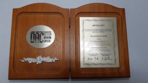
- H. Kitaike, H. Tagawa, S. Xu, R. Zhang, K. Liu, and K. Niitsu, “Design of 0.9-2.6pW 0.1-0.25V 22nm 2-bit Supply-to-Digital Converter Using Always-Activated Supply-Controlled Oscillator and Supply-Dependent-Activation Buffers for Bio-Fuel-Cell-Powered-and-Sensed Time-Stamped Bio-Recording”, ACM/IEEE Asia and South Pacific Design Automation Conference (ASP-DAC), Jan. 2025.
Invited Talks
- 篠原尋史、劉 昆洋、張 瑞琳、徐 舒帆、新津葵一、「バタフライ曲線から考えるSRAMラッチ回路の応用展開」、電子情報通信学会 研究会発表、2025年4月11日
- 新津葵一、「半導体技術と共進化しながら電力・速度間スケーラビリティを可能にする電源・信号電圧一体駆動型ニューロモルフィック集積回路」、一般社団法人電気学会全国大会、2025年3月20日
Awards
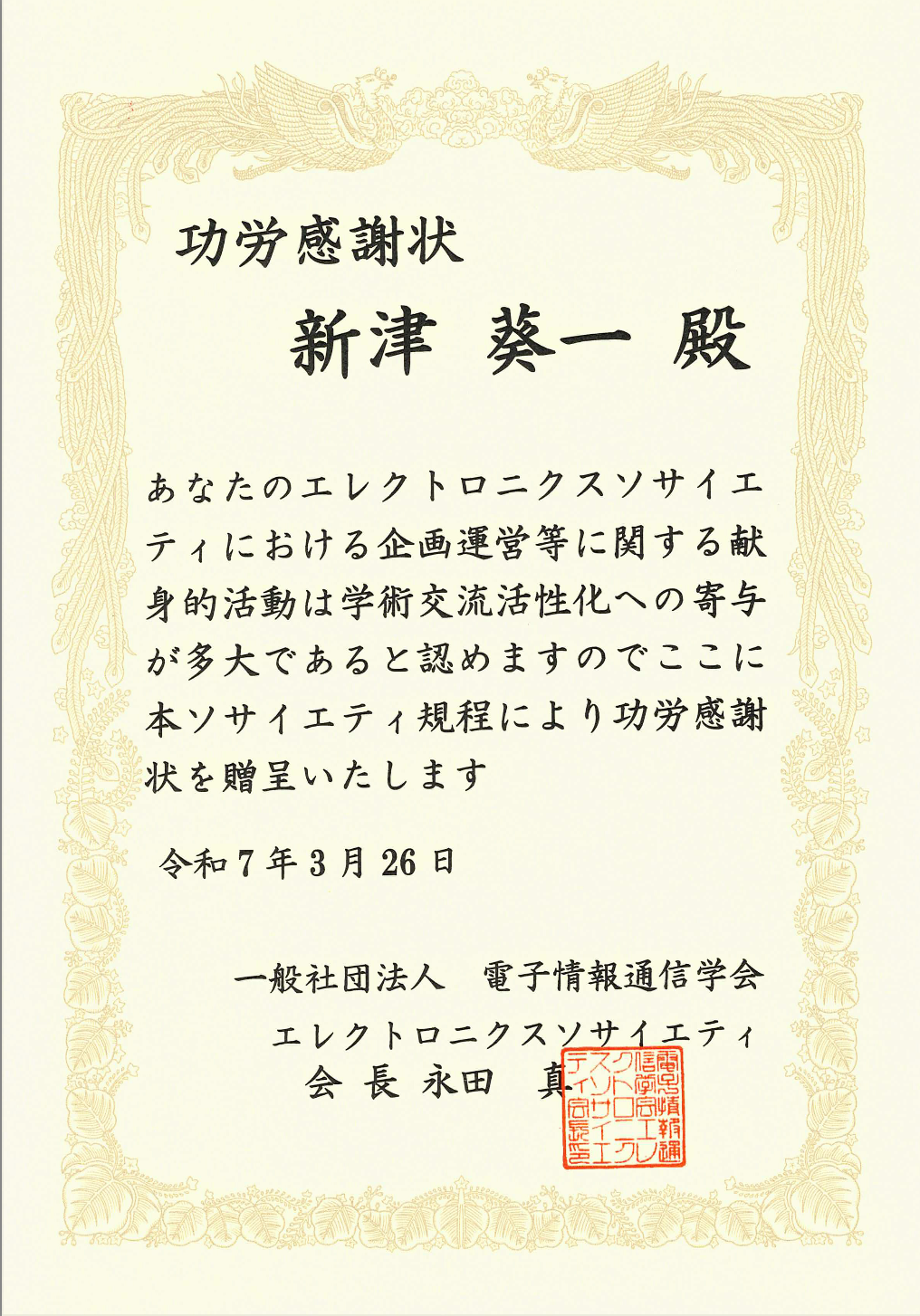
- 新津 葵一、電子情報通信学会エレクトロニクスソサイエティ活動功労表彰受賞、2025年3月26日
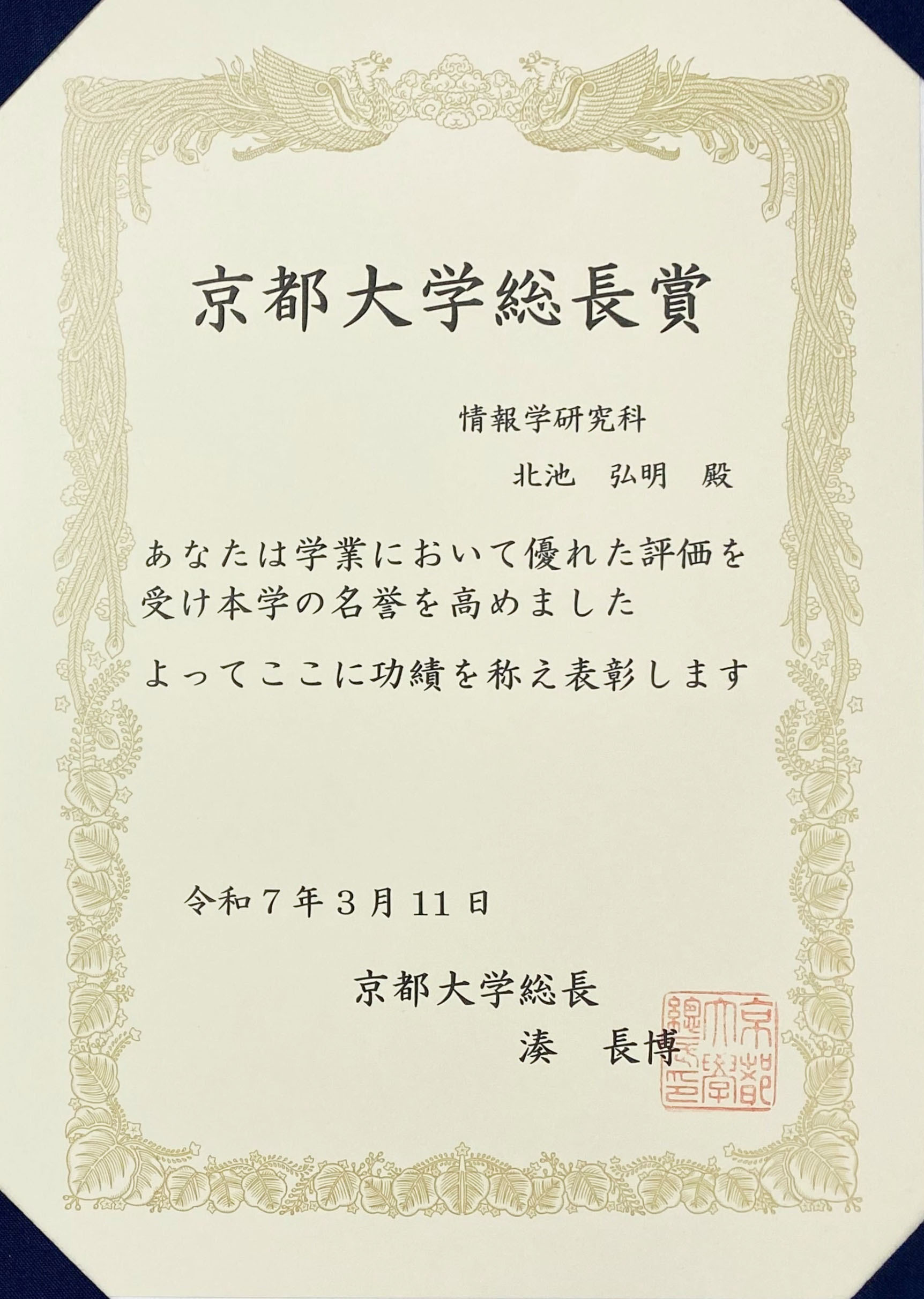
2. 北池 弘明、令和6年度京都大学総長賞、2025年3月11日
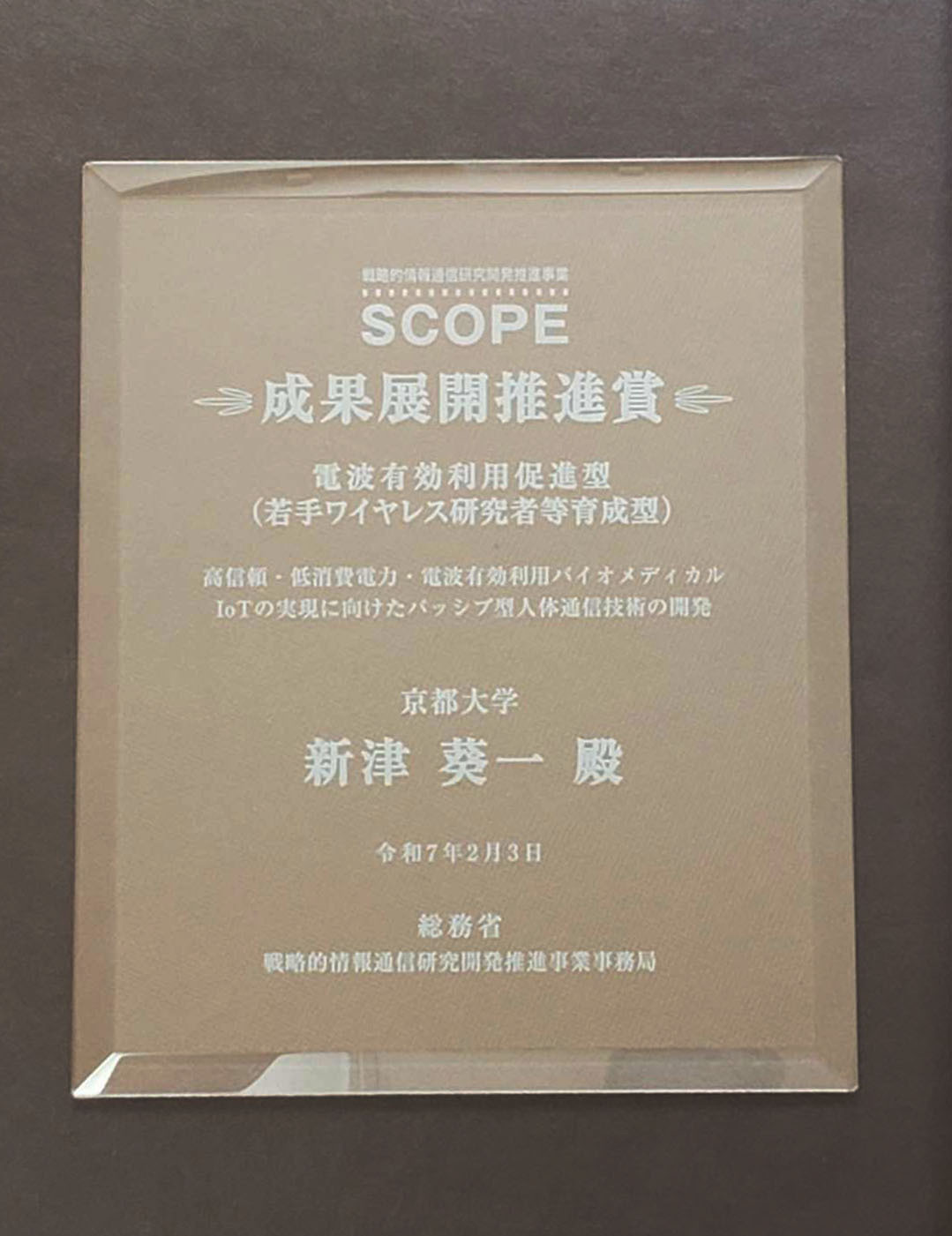
4. 新津 葵一、総務省 戦略的情報通信研究開発推進事業(SCOPE)成果展開推進賞、「高信頼・低消費. 電力・電波有効利用バイオメディカルIoTの実現に向けたパッシブ型人体通信技術の開発」、2025年2月3日
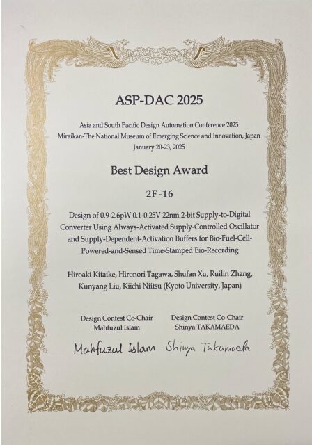
5. Hiroaki Kitaike, Hironori Tagawa, Shufan Xu, Ruilin Zhang, Kunyang Liu and Kiichi Niitsu, “Design of 0.9-2.6p W 0.1-0.25V 22m 2-bit Supply-to-Digital Converter Using Always-Activated Supply-Controlled Oscillator and Supply-Dependent-Activation Buffers for Bio-Fuel-Cell-Powered-and-Sensed Time-Stamped Bio-Recording”, ACM/IEEE Asia and South Pacific Design Automation Conference (ASP-DAC) 2025, Best Design Award, Jan.2025.
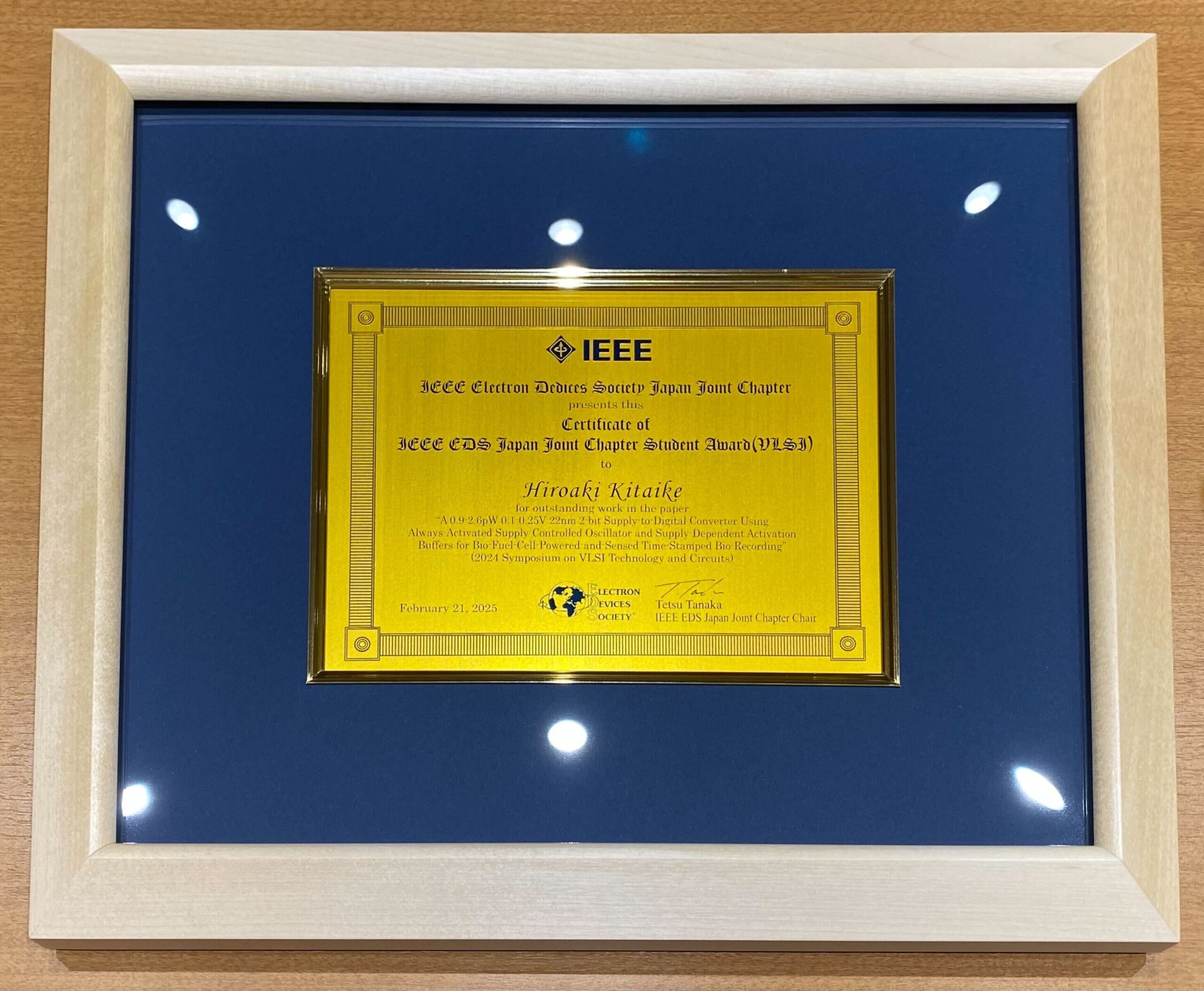
6. Hiroaki Kitaike, “A 0.9-2.6pW 0.1-0.25V 22nm 2-bit Supply-to-Digital Converter Using Always- Activated Supply-Controlled Oscillator and Supply-Dependent-Activation Buffers for Bio-Fuel-Cell-Powered-and-Sensed Time-Stamped Bio-Recording”, IEEE EDS Japan Chapter Student Award (VLSI), Feb.2025.

2024
Journals
- R Zhang, H Zhang, X Wang, Y Ziyang, K Liu, S Nishizawa, K Niitsu, and H Shinohara, “De-correlation and De-bias Post-processing Circuits for True Random Number Generator”, IEEE Transactions on Circuits and Systems I (TCAS-I), vol. 71, no. 11, pp.5187-5199, Jul. 2024.
DOI:10.1109/TCSI.2024.3421663 - X. Wang, R Zhang, K Liu and H. Shinohara, “A 0.116 pJ/bit Latch-Based True Random Number Generator Featuring Static Inverter Selection and Noise Enhancement,” IEEE Transactions on Very Large Scale Integration (VLSI) Systems, vol. 32, no. 3, pp.564-572, Mar. 2024. DOI:10.1109/TVLSI.2023.3328602
International Conferences
- Y. Kiyobayashi, H. Kitaike, J. Nakamura, M. Kaneko, H. Tagawa, K. Okamura, K. Awano, Y. Wu, T. Ono, K. Sakamoto, S. Xu, H. Nakamura, Y. Kimura, K. Liu, R. Zhang, H. Shinohara and K. Niitsu, “A 115mV 300fW 0.24Hz 0.00012mm2 Schmitt-Trigger Ring Oscillator Using Dynamic Leakage Suppression with Cold Start Capability in 22nm CMOS”, IEEE International Conference on Electronics, Circuits and Systems (ICECS 2024), Nov. 2024.
- M. Terauchi, H. Kitaike, H. Tagawa and K. Niitsu, “A 0.04 mm^2 22nm CMOS Fully-Integrated Supply-Modulated OOK Transmitter Using Self-Oscillating Voltage Doubler, Charge Pump, and Voltage Detector”, IEEE International Conference on Electronics, Circuits and Systems (ICECS 2024), Nov. 2024.
- H. Kitaike, H. Tagawa, M. Kaneko, J. Nakamura, S. Xu, R. Zhang, K. Liu, H. Wakatsuchi, K. Takano, H. Shinohara, and K. Niitsu, “A 0.00027 mm2 1.2V 0.089pJ/bit 10Gbps 41.6 GHz Standard-Cell-Based Passive-Less Wireless OOK Transmitter with On-Chip Antenna in 12nm FinFET”, IEEE Nordic Circuits and Systems Conference (NorCAS), Oct. 2024.
- Y. Wu, K. Awano, K. Okamura, T. Ono, K. Sakamoto, H. Kitaike, H. Tagawa, J. Nakamura, M. Kaneko, Y. Kimura, H. Nakamura, S. Xu, R. Zhang, K. Liu, H. Shinohara, and K. Niitsu, “A 2 Hz, 1.2-2 V, 0.22-9 nW, 0.007 mm2 65 nm CMOS Multiple-Output Down-Converter-Less Clock Generator Using Stacked a Ring Oscillator and Frequency Dividers for Scaling-Friendly IoTs”, IEEE Nordic Circuits and Systems Conference (NorCAS), Oct. 2024.
- R. Zhang, H. Zhang, X. Wang, Y. Ziyang, K. Liu, S. Nishizawa, K. Niitsu, and H. Shinohara, “De-correlation and De-bias Post-processing Circuits for True Random Number Generator”, IEEE International Symposium on Integrated Circuits and Systems (ISICAS 2024), Oct. 2024.
- H. Kitaike, M. Inada, M. Terauchi, H. Tagawa, R. Nagai, S. Xu, R. Zhang, K. Liu, and K. Niitsu, “A 0.9-2.6pW 0.1-0.25V 22nm 2-bit Supply-to-Digital Converter Using Always-Activated Supply-Controlled Oscillator and Supply-Dependent-Activation Buffers for Bio-Fuel-Cell-Powered-and-Sensed Time-Stamped Bio-Recording”, IEEE Symposium on VLSI Technology and Circuits (VLSI), pp. 1-2, Jun.2024.
DOI:10.1109/VLSITECHNOLOGYANDCIR46783.2024.10631372 - R. Zhang, X. Jun, J. Liu, X. Wang, S. Xu, K. Liu, S. Nishizawa, K. Niitsu and H. Shinohara, “A Latch-based Stochastic Number Generator for Stochastic Computing of Extended Naïve Bayesian Network”, IEEE International Symposium on VLSI Design, Automation and Test (VLSI-DAT), Apr.2024.
DOI:10.1109/VLSITSA60681.2024.10546408 - K. Niitsu, “A Stand-Alone Continuous Glucose Monitoring Contact Lens Using Glucose-Fuel Cell and CMOS LSI Enabling Memory And Passive-Wireless Readout With Hypoglycemia Predictive Alert”, 17th International Conference on Advanced Technologies & Treatments for Diabetes (ATTD 2024), Mar. 2024.
- H. Kitaike, M. Inada, M. Terauchi, H. Tagawa, R. Nagai, S. Xu, R. Zhang, K. Liu, and K. Niitsu, IEEE International Solid-State Circuits Conference (ISSCC 2024) Student Research Preview, Feb.2024.
- K. Niitsu, K. Fukushima, Y. Hiraoka, H. Urawa, Y. Osaki, M. Kaneko, J. Nakamura, H. Yoshikawa, and Y. Ozawa, “A 65-nm CMOS Millimeter-Wave Ear-Worn Non-Invasive Continuous Glucose Monitoring Chipset Using a 0.17mm² 72mW Transmitter and a 0.75mm² 80mW Direct-Conversion Receiver”, IEEE Latin American Symposium on Circuits and Systems (LASCAS 2024), Feb. 2024.
DOI:10.1109/LASCAS60203.2024.10506119 - G. Chen, A. Tanaka, and K. Niitsu, “A 0.37 V 126 nW 0.29 mm2 65-nm CMOS Biofuel-Cell-Modulated Biosensing System Featuring an FSK-PIM-Combined 2.4 GHz Transmitter for Continuous Glucose Monitoring Contact Lenses”, Asia and South Pacific Design Automation Conference (ASP-DAC 2024), Jan. 2024.
Invited Talks
- 新津葵一、「半導体製造プロセスと共進化する微細適応IoT集積回路とそのバイオ・医療応用展開」、一般社団法人電子情報技術産業協会 Society5.0/SDGsを加速するセンシング技術分科会 、2024年11月26日
- 新津葵一、「先端半導体活用低電力IoTに向けた電源電圧デジタル変換集積回路設計技術」、『モータやパワーエレクトロニクスを支える回路技術』第22回大学発シーズマッチングセミナー、2024年11月22日
- 新津葵一、「半導体共進化微細IoTに向けた微細化適応半導体集積回路設計ー発電センシング一体型集積センサに向けた0.1V 0.9pW 22nm CMOS電源環境適応型電源電圧デジタル変換回路ー」日本学術振興会 R025先進薄膜界面機能創成委員会 第20回研究会、2024年8月22日
- 新津葵一、「半導体共進化微細IoTに向けた集積回路設計技術 ~ 発電・センシング一体型バイオ集積IoTに向けた 常時オン発振器と異なるしきい値電源電圧を有する信号バッファ群を用いた 0.9-2.6pW 0.1-0.25V 2ビット 22nm CMOS電源電圧・デジタル変換回路 ~」電子情報通信学会 研究会、2024年8月5日
- 新津葵一、「バイオメディカル IoT を支える電力自立センシング半導体集積回路システム」、電気三学会関西支部 専門講習会、2024年6月25日
- [Invited]K. Niitsu, “Bio-fuel-cell-powered-and-sensed Biomedical IoTs”, 2024 IEEE the 13th International Conference on Communications, Circuits, and Systems (ICCCAS) ,May. 2024.(中国・廈門市)
Awards
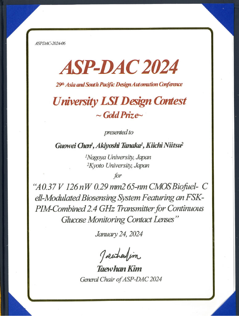
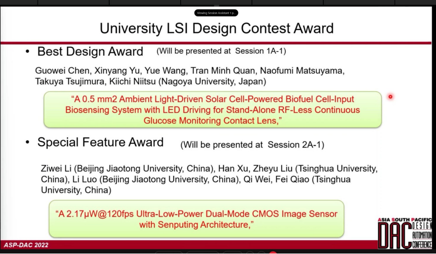
- Guowei Chen, Akiyoshi Tanaka and Kiichi Niitsu, “A0.37V 126nW 0.29mm265-nm CMOS Biofuel-Cell-Modulated Biosensing System Featuring an FSK-PIM-Combined 2.4 GHz Transmitter for Continuous Glucose Monitoring Contact Lenses, ” 29th Asia and South Pacific Design Automation Conference, University LSI Design Contest~Gold Prize~, Jan.2024.

Patents
- 新津 葵一、「アナログデジタル変換回路及びそれを備えた半導体チップ」特願2024-149947(出願日:2024年8月30日)出願中
Press Release
- 新津 葵一、劉 昆洋、張 瑞琳、北池 弘明、田川 宏紀、「環境適応電源・デジタル変換半導体集積回路の開発に成功〜22nmで実証、体内で自律動作するIoTの開発へ〜」、国立研究開発法人 科学技術振興機構・京都大学、2024年6月17日
https://www.jst.go.jp/pr/announce/20240617/index.html
2023
Journals
- S. Imai, H. Homma, K. Takimoto, M. Tanikawa, J. Nakamura, M.Kaneko, Y. Osaki, K. Niitsu, C. Yongzhi, A. A. Fathnan,and H. Wakatsuchi, “Design guidelines for the SPICE parameters of waveform-selective metasurfaces varying with the incident pulse width at a constant oscillation frequency”, Scientific Reports, vol. 13, no. 7202, pp.9, May. 2023.
DOI: https://doi.org/10.1038/s41598-023-34112-z
International Conferences
- R. Nagai, M. Inada, H. Kitaike, H. Tagawa, M. Terauchi, T. M. Quan, H. Nakamura, and K. Niitsu, “A Continuous Multiple-Timestep Blood Glucose Level Prediction System Using Stacked LSTM for High-Accuracy Hypoglycemia Alerting in Smart Contact Lenses,” IEEE International Conference on Data Science and Engineering in Healthcare, Medicine & Biology (DSEHMB 2023), Dec. 2023.
- A. Tanaka, G. Chen, and K. Niitsu, “A 0.063-mm^2 1.75-nW Biofuel Cell-Input Biosensing/Data-Storing System with 5.5-GHz Wireless Backscatter Data-Readout in 65-nm CMOS for Self-Powered Smart Contact Lenses,” 2023 IEEE Biomedical Circuits and Systems Conference, Oct. 2023.
DOI:10.1109/BioCAS58349.2023.10388802 - K. Niitsu, J. Nakamura, M. Kaneko, Y. Osaki and H. Wakatsuchi, “A 351pW Stand-By Power 0.017mm2 37.4GHz LC Oscillator-Based OOK Transmitter Using Low-Leakage Switch in 22nm Planer CMOS,” International Conference on Solid State Devices and Materials (SSDM2023), Sep. 2023.
- R. Zhang, H. Zhang, X, Wang, Y. Ziyang, K. Liu and H. Shinohara, “Practical Markov Chain and Von Neumann based Post-processing Circuits for True Random Number Generators,” 2023 IEEE 66th International Midwest Symposium on Circuits and Systems (MWSCAS), Aug. 2023. DOI:10.1109/MWSCAS57524.2023.10406056
- G. Chen, A. Tanaka and K. Niitsu, “A Battery-Less 0.37 V 126 nW 0.29 mm2 65-nm CMOS Biofuel-Cell-Modulated Biosensing System Featuring an FSK-PIM-Combined 2.4 GHz Transmitter for Continuous Glucose Monitoring Contact Lenses,” IEEE Symposium on Circuits and Systems (ISCAS 2023), May. 2023.
DOI:10.1109/ISCAS46773.2023.10182119 - K. Liu, Y. Tang, S. Xu, R, Zhang and H. Shinohara, “A 100-Bit-Output Modeling Attack-Resistant SPN Strong PUF with Uniform and High-Randomness Response,” 2023 IEEE Custom Integrated Circuits Conference (CICC), Apr. 2023. DOI:10.1109/CICC57935.2023.10121278
- K. Liu, Y. Tang, S. Xu and H. Shinohara, “VSS-Bias-Based Measurement of Random Telegraph Noise in Hybrid SRAM PUF after Hot Carrier Injection Burn-in,” 2023 35th International Conference on Microelectronic Test Structure (ICMTS), Mar. 2023. DOI:10.1109/ICMTS55420.2023.10094138
- S. Xu, K. Liu, Y. Tang, R. Zhang and H. Shinohara, “Effect of Quadruple Size Transistor on SRAM Physically Unclonable Function Stabilized by Hot Carrier Injection,” 2023 35th International Conference on Microelectronic Test Structure (ICMTS), Mar. 2023. DOI:10.1109/ICMTS55420.2023.10094187
Domestic Conference Papers
- 稲田 雅治、北池 弘明、田川 宏紀、寺内 充、長井 亮輔、伊藤 榛一、田中 彬義、大崎 雄也、金子 優哉、中村 迅、新津 葵一、「バイオ医療IoTに向けた分解能・サイズ・電力スケーラブルなサブテラヘルツ帯ラベルフリー3次元センサアレイの12nmFinFET/22nmCMOSでの理論的・実験的検証」、LSIとシステムのワークショップ、2023年5月10日
Invited Talks
- 新津葵一、「データ科学と半導体集積回路の進化が切り拓く糖尿病医療に向けたIoT〜低血糖予知機能搭載コンタクト型・耳装着型持続血糖モニタリングの研究開発〜」、第8回日本糖尿病・生活習慣病ヒューマンデータ学会年次学術集会、2023年12月1日
- [Invited]K Niitsu, “Integrating Iots into Our Life : Energy-Efficient COMS-Enabled Biomedical Iot Systems Improving Our Health,” The 13th International Conference on the Internet of Things, Nov.2023. (名古屋市)
- 新津 葵一、「半導体集積回路と生命医科学における進化の協奏が織り成す生体内サイバネテック・アバター」第41回日本ロボット学会学術講演会 2023年9月11日
- 新津 葵一、「最先端半導体集積回路設計技術と分析化学の融合による未来のヘルスケアIoT ~単独自立動作可能な持続血糖モニタリングコンタクトレンズの開発」日本分析化学会 第83回分析化学討論会 2023年5月20日
- 新津 葵一、「半導体集積回路の進化が切り拓くバイオ・医療応用IoTの研究開発と将来展望
~涙液糖発電センシングによる単独自立動作持続血糖モニタリングコンタクトの開発~」本顎口腔機能学会 第69回学術大会 2023年4月22日 - 新津 葵一、「半導体集積回路の微細化が切り拓くTinyCMOS技術とその応用展開~涙液糖発電セン シングで自立動作可能な持続血糖モニタリングコンタクトレンズ」電子情報通信学会 短距離無線通信研究会(SRW) 2023年1月16日
Awards
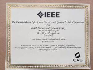
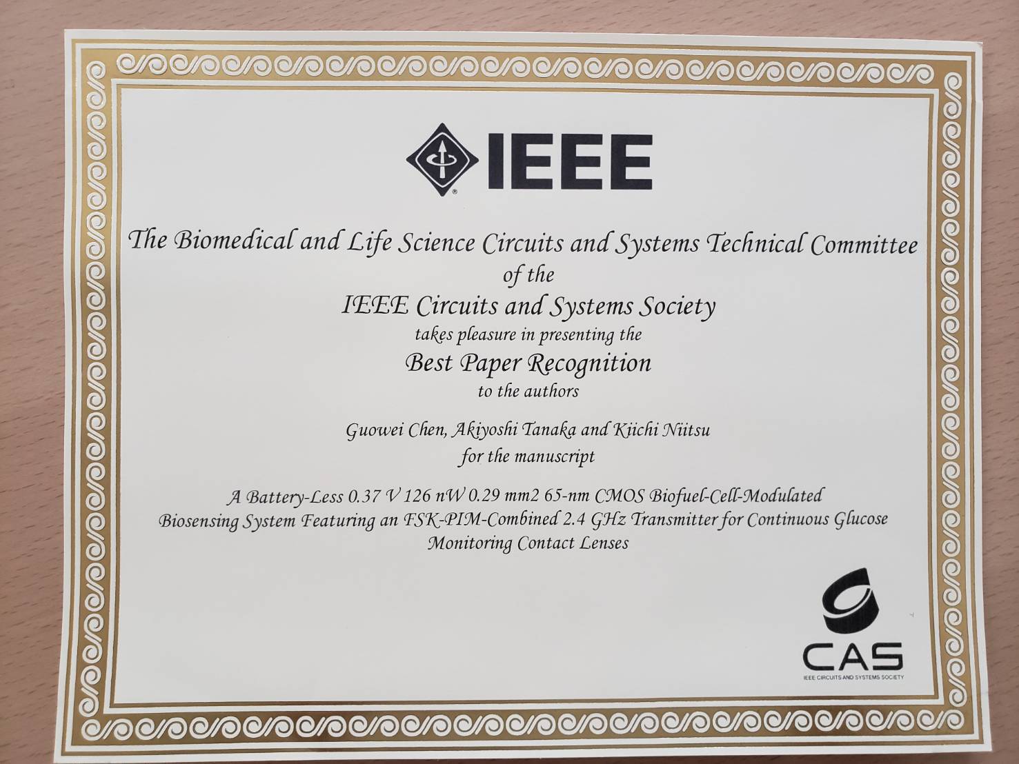
- Guowei Chen, Akiyoshi Tanaka and Kiichi Niitsu, A Battery-Less 0.37 V 126 nW 0.29 mm2 65-nm CMOS Biofuel-Cell-Modulated Biosensing System Featuring an FSK-PIM-Combined 2.4 GHz Transmitter for Continuous Glucose Monitoring Contact Lenses, IEEE Circuits and Systems Society, Best Paper Recognition, May. 2023.
- 稲田 雅治、北池 弘明、田川 宏紀、寺内 充、長井 亮輔、 伊藤 榛一、田中 彬義、 大崎 雄也、金子優哉、中村 迅、新津 葵一、LSIとシステムのワークショップ最優秀ポスター賞(学生部門)、『バイオ医療IoTに向けた分解能・サイズ・電力スケーラブルなサブテラヘルツ帯ラベルフリー3次元センサアレイの12nmFinFET/22nmCMOSでの理論的・実験的検証』、2023年5月
- 新津 葵一、「バイオ発電と省電力半導体集積回路を用いた電力自立ヘルスケアIoT」、第10回京都SMI中辻賞(特定非営利活動法人 京都SMI)、2023年1月 第10回京都SMI中辻賞の受賞者決定 | 特定非営利活動法人 京都SMI (kyoto-smi.or.jp)
Patents
- 山中 俊郎、新井 史人、伊藤 大知、藤城 光弘、辻 陽介、新津 葵一、「腸管壁保持装置」特願2023-144775、特開2025-37688(出願日:2023年9月6日)出願中
2022
Journals
- R. Zhang, X. Wang, K. Liu and H. Shinohara, “A 0.186-pJ per Bit Latch-Based True Random Number Generator Featuring Mismatch Compensation and Random Noise Enhancement,” IEEE Journal of Solid-State Circuits, vol. 57, pp.2498-2508, Aug. 2022.
DOI: 10.1109/JSSC.2021.3137312 - A. Tanaka, G. Chen, and K. Niitsu, “A 4.5-mW 22-nm CMOS Label-Free Frequency-Shift 3×3×2 3D Biosensor Array Using Vertically-Stacked 60-GHz LC Oscillators”, IEEE Transactions on Circuits and Systems II: Express Briefs ( Early Access ), Jun. 2022.
DOI: https://doi.org/10.1109/TCSII.2022.3185542 - G. Chen, X. Chen and K. Niitsu, “Design and Experimental Verification of A 2.1 nW 0.018 mm2 Slope ADC-Based Supply Voltage Monitor for Biofuel-Cell-Powered Supply-Sensing Systems in 180-nm CMOS”, IEICE Transactions, vol. E105.C, no. 10, pp. 565-570, Mar. 2022.
DOI: https://doi.org/10.1587/transele.2021CTS0001 - G. Chen, Y. Wang, T. M. Quan, N. Matsuyama, T. Tsujimura and K. Niitsu, “ A 0.5 mm2 Solar Cell-Powered Biofuel Cell-Input Biosensing System with LED Driving for Stand-Alone RF-Less Continuous Glucose Monitoring Contact Lens”, IEEE Solid-State Circuits Letters, vol. 5, pp. 41–44, Feb. 2022.
DOI: https://doi.org/10.1109/LSSC.2022.3151904
International Conferences
- Y. Hayashi and K. Niitsu, “A 22nm CMOS 1.25V 29pW 0.000013 mm2 Supply Voltage Detector Using Stacked 3 Thick-Gate-Oxide PMOSs and Dynamic Leakage Suppression Buffer”, International Conference on Solid State Devices and Materials (SSDM 2022), Sep. 2022.
- A. Tanaka, G. Chen and K. Niitsu, “A 4.5-mW 22-nm CMOS Label-Free Frequency-Shift 3×3×2 3D Biosensor Array Using Vertically-Stacked 60-GHz LC Oscillators”, IEEE International Symposium on Integrated Circuits and Systems (ISICAS 2022), Oct. 2022.
DOI:10.1109/TCSII.2022.3185542 - K. Liu, G. Li, Z. Fu, X. Wang and H. Shinohara, “A 2.17-pJ/b 5b-Response Attack-Resistant Strong PUF with Enhanced Statistical Performance,” ESSCIRC 2022- IEEE 48th European Solid State Circuits Conference (ESSCIRC), Sep. 2022.
DOI:10.1109/ESSCIRC55480.2022.9911472 - S. Ito, A. Tanaka, G. Chen, X. Chen and K. Niitsu, “A 0.00023 mm2 1.2V 0.48mW 18GHz Passive-Less Digital Wireless Transmitter with On-Chip Antenna in 22nm Bulk CMOS”, 2022 IEEE International Midwest Symposium on Circuits and Systems, Aug. 2022.
DOI:10.1109/MWSCAS54063.2022.9859365 - A. Tanaka, G. Chen and K. Niitsu, “A 4.8-mW Label-free Frequency-shift 3×3×2 3D Biosensor Array with Vertically-stacked60-GHz LC Oscillators in 22-nm CMOS”, 2022 IEEE International Midwest Symposium on Circuits and Systems, Aug. 2022.
DOI: 10.1109/MWSCAS54063.2022.9859351 - K. Liu, K. Takeuchi and H. Shinohara, “Statistical Modeling of SRAM PUF Cell Mismatch Shift Distribution After Hot Carrier Injection Burn-In,” 2022 IEEE 34th International Conference on Microelectronic Test Structures (ICMTS), Apr. 2022.
DOI: 10.1109/ICMTS50340.2022.9898258 - X. Wang, R. Zhang, Y. Wang, K, Liu, X, Wang and H. Shinohara, “A 0.116pJ/bit Latch-Based True Random Number Generator with Static Inverter Selection and Noise Enhancement,” 2022 International Symposium on VLSI Design, Automation and Test (VLSI-DAT), Apr. 2022.
DOI: 10.1109/VLSI-DAT54769.2022.9768078 - T. Tsujimura, G. Chen, Y. Hayashi, S. Kato and K. Niitsu, “Design of Wideband CMOS Biosensor with Active-Inductor-Based VCO for DetectingCTCs and Exosomes”, ISPlasma2022/IC-PLANTS2022, Mar. 2022.
- T. Tsujimura and K. Niitsu, “CMOS-Based Biosensor Using Broadband Tunable Active-Inductor-Based VCO with γ-Dispersion for Detecting CTCs and Exosomes”, IEEE Latin American Symposium on Circuits and Systems (LASCAS 2022), Mar. 2022.
- H. Duong, G. Chen and K. Niitsu, “22nm CMOS pW Standby Power Flip-Flops with/without Security using Dynamic Leakage Suppression Logic”, IEEE Latin American Symposium on Circuits and Systems (LASCAS 2022), Mar. 2022.
DOI:10.1109/LASCAS53948.2022.9789041 - S. Kato, G. Chen and K. Niitsu “An Ultra-Low Power 22 nm Self-Oscillating Voltage Doubler With Dynamic Leakage-Suppression Logic”, IEEE Latin American Symposium on Circuits and Systems (LASCAS 2022), Mar. 2022.
DOI: 10.1109/LASCAS53948.2022.9789081 - X. Chen, G. Chen, X. Yu, Y. Wang and K. Niitsu, “A 52.3% Peak Efficiency 22nm CMOS Low-Power Light-Adaptive Self-Oscillating Voltage Doubler Using Scalable Dynamic Leakage-Suppression Logic”, IEEE Latin American Symposium on Circuits and Systems (LASCAS 2022), Mar. 2022.
DOI: 10.1109/LASCAS53948.2022.9789056 - G. Chen, X. Yu, Y. Wang, T. M. Quan, N. Matsuyama, T. Tsujimura and K. Niitsu, “ A 0.5 mm2 Ambient Light-Driven Solar Cell-Powered Biofuel Cell-Input Biosensing System with LED Driving for Stand-Alone RF-Less Continuous Glucose Monitoring Contact Lens”, Asia and South Pacific Design Automation Conference – University Design Contest (ASP-DAC UDC 2022), Jan. 2022.
DOI:10.1109/ASP-DAC52403.2022.9712523
Invited Talks
- [Tutorial]K. Niitsu, “Energy/Data-Autonomous AIoT CMOS Integrated Platform Using Localized Energy/Data Generation and Consumption”, 2022 IEEE 16th International Conference on Solid-State and Integrated Circuit Technology Tutorial Sessions, Oct. 2022.(中国・南京市)
- 新津 葵一、「半導体集積回路の微細化が切り拓くスケーラブル・バイオイメージングの現状と展望」第31回日本バイオイメージング学会学術集会、2022年9月4日
- 新津 葵一、「高エネルギー効率特定用途半導体集積回路とバイオ発電素子を用いた 単独自立型持続血糖モニタリングコンタクトレンズ」日本学術振興会 R025先進薄膜界面機能創成委員会 第8回研究会、2022年4月13日
- 新津 葵一、「最先端半導体集積回路エレクトロニクスが切り拓く非侵襲血糖モニタリング技術~涙液糖発電を用いた単独動作持続血糖モニタリングコンタクトレンズ・ミリ波帯を用いた耳装着クリップ型モニタの開発~」第9回 Digital Medical Innovation Lab.主催 医療DX講演会、2022年2月25日
Awards
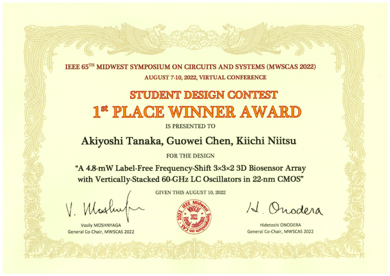
- Akiyoshi Tanaka, Guowei Chen and Kiichi Niitsu, “A 4.8-mW Label-free Frequency-shift 3×3×2 3D Biosensor Array with Vertically-stacked 60-GHz LC Oscillators in 22-nm CMOS,” 2022 IEEE 65th IEEE MWSCAS 2022 Student Design Contest 1st prize, Jul 2022.
- 新津 葵一、令和3年度SCOPE研究開発奨励賞(総務省:戦略的情報通信研究開発推進事業事務局)、「高信頼・低消費電力・電波有効利用バイオメディカル IoT の実現に向けたパッシブ型人体通信技術の開発」、2022年2月3日
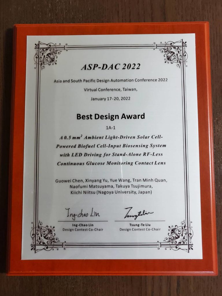
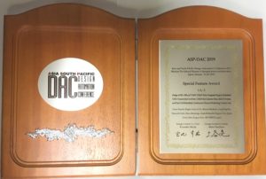
- Guowei Chen, Xinyang Yu, Yue Wang, Tran Minh Quan, Naofumi Matsuyama, Takuya Tsujimura, Kiichi Niitsu, A 0.5 mm2 Ambient Light-Driven Solar Cell-Powered Biofuel Cell-Input Biosensing System with LED Driving for Stand-Alone RF-Less Continuous Glucose Monitoring Contact Lens, ASP-DAC 2022 Best Design Award Jan. 20, 2022.
Patents
- K.Niitsu, “Measuring device, container device, and measuring system”, No.11347083, (米国出願番号:17/052,583), (出願日:2020年11月03日) 登録
Google特許:https://patents.google.com/patent/US11347083B2/en?oq=US+11347083
(PDFダウンロード)
2021
Journals
- G. Chen and K. Niitsu, “A Solar-Cell-Assisted, 99% Biofuel Cell Area Reduced, Biofuel-Cell-Powered Wireless Biosensing System in 65nm CMOS for Continuous Glucose Monitoring Contact Lenses”, IEICE Transactions on Electronics, vol. E105.C, no.7, pp.343-348, Dec. 2021.
DOI: https://doi.org/10.1587/transele.2021CDS0002 - Md. Z. Islam, A. Watthanaphanit, S. Chae, K. Niitsu and N. Saito, “Structure and properties of nanocarbons-encapsulated WC synthesized by solution plasma process in palm oils”, Materials Express Journal, vol 11, no 9, pp. 1602-1607(6), Sep. 2021.
DOI: https://doi.org/10.1166/mex.2021.2034 - Md. Z. Islam, A. Watthanaphanit, S. Chae, K. Niitsu and N. Saito, “High electrical conductivity and oxidation reduction reaction activity of tungsten carbide/carbon nanocomposite synthesized from palm oil by solution plasma process”, Materials Express Journal, vol 11, no 9, pp. 1587-1593(7), Sep. 2021.
DOI: https://doi.org/10.1166/mex.2021.2035 - K. Liu, X. Chen, H. Pu and H. Shinohara, “A 0.5-V Hybrid SRAM Physically Unclonable Function Using Hot Carrier Injection Burn-In for Stability Reinforcement”, IEEE Journal of Solid-State Circuits, vol.56, no 7, pp. 2193-2204, Jul. 2021.
DOI: 10.1109/JSSC.2020.3035207 - S. Jodo, T. Iwaki, K. Uchiyama, Md. Islam, K. Kataoka, Y. Hayasaka, J. Imaoka, M. Yamamoto, K. Niitsu, “A simple gate driver design for GaN-based switching devices with improved surge voltage and switching loss at 1 MHz operation,” Japanese Journal of Applied Physics, vol.60, no. SAAD02, Jan. 2021.
DOI:https://doi.org/10.35848/1347-4065/abbdc7
International Conferences
- Y. Hayashi, G. Chen, K Niitsu, ”A FSK Wireless Transmitter in 22-nm CMOS for Biomedical Applications with On-Chip Photodiode,” in Proc. IEICE International Conference on Emerging Technologies for Communications (ICETC), p. 1, Dec. 2021.
DOI:10.34385/proc.68.P4-1 - A. Tanaka, G. Chen and K. Niitsu, “A 0.2V 0.97nW 0.011mm^2 Fully-Passive mHBC Tag Using Intermediate Interference Modulation in 65nm CMOS”, IEEE International Conference on Electronics, Circuits & Systems (ICECS 2021), Nov. 2021.
DOI:10.1109/ICECS53924.2021.9665542 - A. Tanaka, G. Chen and K. Niitsu, “A 4.8mW 22nm CMOS Fully-Integrated 60-GHz 3×3×2 3D Frequency-Shift Biosensor Array Using Vertically-Stacked LC Oscillators”, IEEE International Conference on Electronics, Circuits & Systems (ICECS 2021), Nov. 2021.
DOI: 10.1109/ICECS53924.2021.9665493 - X. Yu, G. Chen, Y. Wang, X. Chen and K. Niitsu, “A 65-nm CMOS 0.4 V 49.6 nW Voltage Monitor for Small-Form-Factor Biomedical IoT Applications”, in Proc. 2021 IEEE Asia Pacific Conference on Postgraduate Research in Microelectronics and Electronics (PrimeAsia), Sep. 2021.
DOI:10.1109/PrimeAsia51450.2021.9701468 - Y. Wang, G. Chen, X. Yu, X. Chen and K. Niitsu, “A 22nm CMOS 0.2V 13.3nW 16T SRAM Using Dynamic Leakage Suppression and Half-Selected Free Technique”, in Proc. IEEE Asia Pacific Conference on Circuits and Systems (APCCAS 2021), Sep. 2021.
DOI:10.1109/APCCAS51387.2021.9687693 - G. Chen, X. Yu, Y. Wang, T. M. Quan, N. Matsuyama, T. Tsujimura, M. Z. Islam and K. Niitsu, “A 0.5 mm2 0.31 V/0.39 V 28 nW/144 nW 65 nm CMOS Solar Cell-Powered Biofuel Cell-Input Biosensing System with PIM/PDM LED Driving for Stand-Alone RF-Less Continuous Glucose Monitoring Contact Lens”, in Proc. IEEE 47th European Solid State Circuits Conference (ESSCIRC 2021), in Proc. IEEE 50st European Solid-State Device Researech Conference (ESSDERC 2021), Sep. 2021.
DOI:10.1109/ESSCIRC53450.2021.9567771,10.1109/ESSDERC53440.2021.9631770 - R. Zhang, X. Wang, L. Wang, X. Chen, F. Y. Liu and H. Shinohara, “A 0.186-pJ per Bit Latch-Based True Random Number Generator with Mismatch Compensation and Random Noise Enhancement”, 2021 Symposium on VLSI Circuits, Jun. 2021.
DOI:10.23919/VLSICircuits52068.2021.9492474 - S. Jodo and K. Niitsu, “Design of CMOS Gate Driver Circuit for Power Devices with Smaller Switching Loss Using Bootstrap Technique” ISPlasma2021, Mar. 2021.
- K. Liu, Z. Fu, G. Li, H. Pu, Z. Guan, X. Wang, X. Chen and H. Shinohara, “36.3 A Modeling Attack Resilient Strong PUF with Feedback-SPN Structure Having <0.73% Bit Error Rate Through In-Cell Hot-Carrier Injection Burn-In”, 2021 IEEE International Solid-State Circuits Conference (ISSCC), Feb. 2021. DOI: 10.1109/ISSCC42613.2021.9365942
- S. Murakami, T. Tsujimura, G. Chen, M. Z. Islam and K. Niitsu, “Simulation Comparison of Two Tyeps of CMOS-Based Biosensors for Detecting CTCs and Exosomes”, ISPlasma2021, Jan. 2021.
- T. Tsujimura, S. Murakami, G. Chen, M. Islam, and K. Niitsu, “Design and Simulation of 33 GHz 65-nm-CMOS Small-Formfactor Direct-Conversion Receiver for Non-Invasive Continuous Glucose Monitoring” ISPlasma2021, Jan. 2021.
Invited Talks
- 新津葵一、「サブ平方mm/サブnW半導体集積回路及び糖発電素子を用いた 環境適応自立駆動型持続血糖モニタIoTスマートコンタクトレンズ」第85回半導体・集積回路技術シンポジウム、2021年8月31日
- 新津葵一、「小児糖尿病医療に資する次世代のAI×IoT技術~単独動作可能AI機能付き持続血糖モニタリングコンタクトレンズの研究開発~」埼玉県小児糖尿懇話会、2021年2月24日
- 新津葵一、「低侵襲がん医療に資するリキッドバイオプシーに向けたCTC・エクソソーム検出ミリ波帯CMOSバイオセンサ集積回路」高速・高周波集積回路の新分野展開と高度化技術調査専門委員会、2021年1月22日
Awards
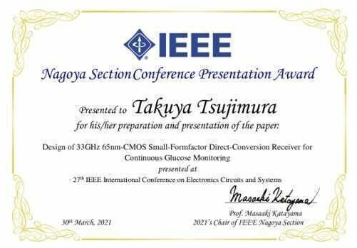
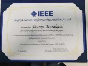
1.辻村 拓也, 2021年IEEE名古屋支部国際会議研究発表賞受賞 2021年3月
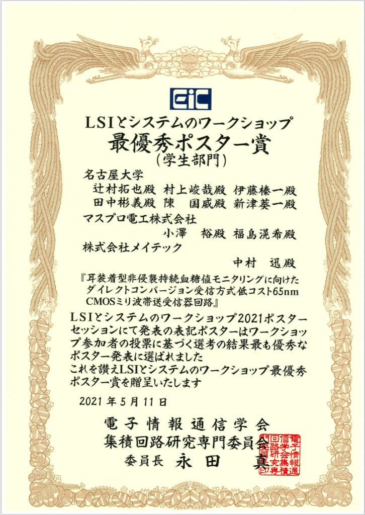
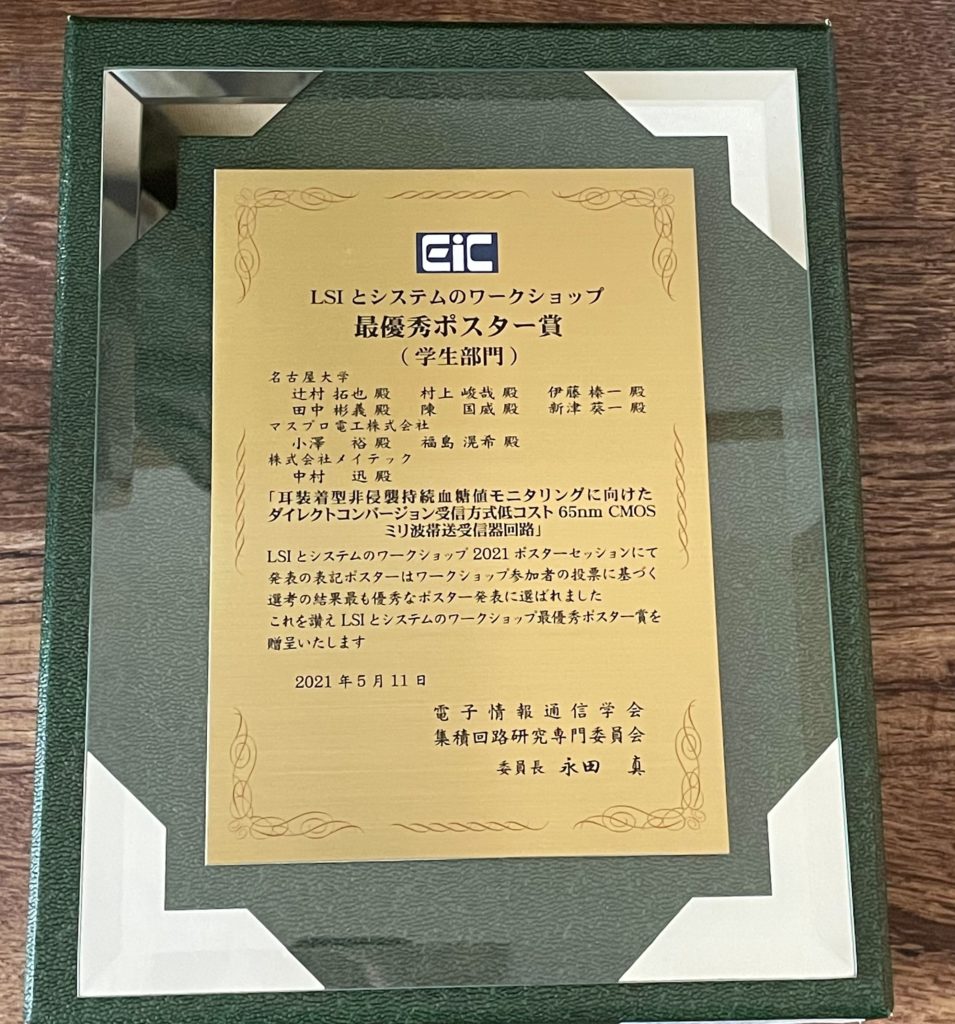
2.辻村 拓也, 村上 峻哉, 伊藤 榛一,田中 彬義, 陳 国威, 新津 葵一, (マスプロ電工株式会社)小澤 裕, 福島 滉希, (株式会社メイテック)中村 迅,「耳装着型非侵襲持続血糖値モニタリングに向けたダイレクトコンバージョン受信方式低コスト65nm CMOSミリ波帯送受信器回路」, LSIとシステムのワークショップ2021最優秀ポスター賞(学生部門)2021.5.11
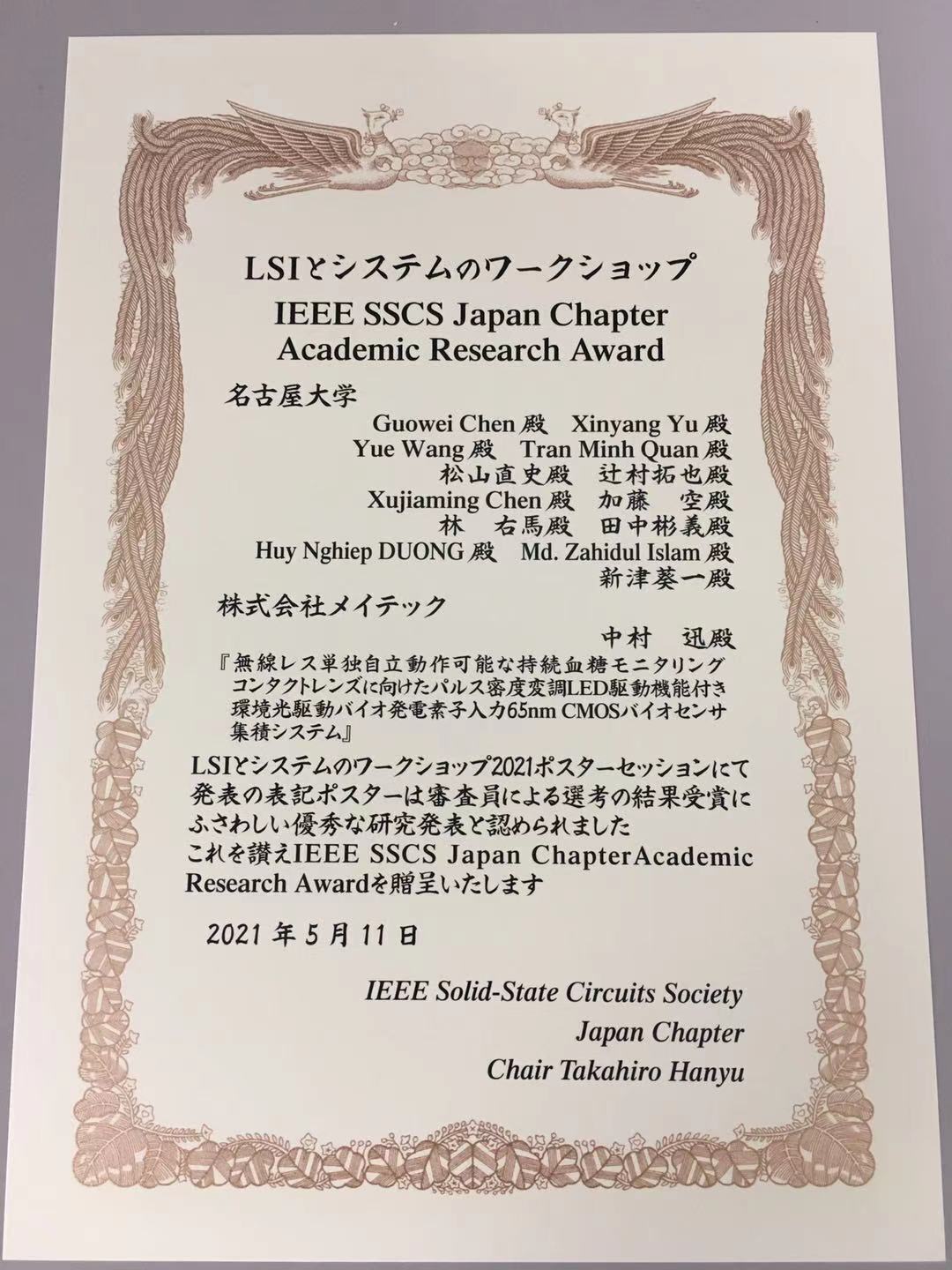
3.陳 国威(Guowei Chen), Xinyang Yu, Yue Wang, Tran Minh Quan, 松山 直史, 辻村 拓也, Xujiaming Chen, 加藤 空, 林 右馬, 田中 彬義, Huy Nghiep DUONG, Md. Zahidul Islam, 新津 葵一, (株式会社メイテック)中村 迅,「無線レス単独自立動作可能な持続血糖モニタリングコンタクトレンズに向けたパルス密度変調LED駆動機能付き環境光駆動バイオ発電素子入力65nm CMOSバイオセンサ集積システム」,LSIとシステムのワークショップ2021 IEEE SSCS Japan Chapter Academic Research Award 2021.5.11
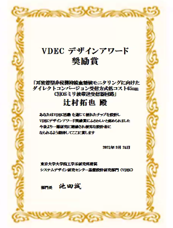
4.辻村 拓也,「耳装着型非侵襲持続血糖値モニタリングに向けたダイレクトコンバージョン受信方式低コスト65nm CMOSミリ波帯送受信器回路」, d.lab-VDECデザイナーズフォーラム2021 2021年9月
Japanese Journals
- 新津 葵一、「自立駆動型コンタクトレンズ型センサ」、機能材料2021年3月号、CMC出版、2021年3月7日
Books and Articles
- 新津 葵一、「テレワーク社会を支える自立駆動型コンタクトレンズ型センサ」、テレワーク社会を支えるリモートセンシング、CMC出版、2021年4月26日
2020
Journals
- M. Z. Islam, S. Arata, K. Hayashi, X. Ge, N. Matsuyama, S. Murakami, A. Kobayashi, H. Cheng, and K. Niitsu, “Design of an electrical equivalent circuit model of a CMOS-process-compatible glucose fuel cell as a power supply in integrated circuits” Nanoscience and Nanotechnology Letters, Vol.12, no.5, pp.642-645, May. 2020.
DOI:https://doi.org/10.1166/nnl.2020.3146 - A. Kobayashi, and K. Niitsu “Low-Voltage Gate-Leakage-Based Timer Using an Amplifier-Less Replica-Bias Switching Technique in 55-nm DDC CMOS” . IEEE Open Journal of Circuits and Systems(OJCAS 2020), vol.1, pp. 107 – 114, Jul. 2020.
DOI: 10.1109/OJCAS.2020.3007393 - M. Z. Islam, S. Arata, K. Hayashi, A. Kobayashi, Y. Momoi and K. Niitsu, “Biomedical Application Via Implantable Devices By CMOS-Compatible Glucose Fuel Cells Using Carbon Nano Horn”, ECS Transactions” (ECST) vol. 97, no. 7, pp. 311, 2020.
DOI:https://doi.org/10.1149/09707.0311ecst - G. Xu, K. Hayashi, S. Arata, S. Murakami, D. C. Bui, A. Kobayashi and K. Niitsu, “Design and Theoretical Analysis of Bit Error Rate (BER)-modulated Inductive-coupling Transceiver Using Dynamic Intermediate Interference Control Technique for Low-power Communication”, Sensors and Materials, Vol 32, no 8, pp. 2631-2639, Aug. 2020.
DOI:https://doi.org/10.18494/SAM.2020.2558 - M. Z. Islam, N. Matsuyama, G. Chen, A. Kobayashi, Y. Momoi and K. Niitsu, “A Needle-type complementary metal oxide semiconductor-compatible glucose fuel cell fabricated by carbon nanohorns for biomedical applications”, Electrochemistry, vol. 88, no. 4, pp. 333–335, May. 2020.
DOI:https://doi.org/10.5796/electrochemistry.20-00044 - S. Murakami, K. Hayashi, S. Arata, G. Xu, C. D. Bui, A. Kobayashi, and K. Niitsu, “Design and Verification of a Stochastic Oscillator Using Multiple Ring Oscillators and OR Gate for Low Voltage Operation in 65 nm CMOS”, Sensors and Materials, vol 32, no 8, pp. 2607-2614, Aug. 2020.
DOI:https://doi.org/10.18494/SAM.2020.2496 - M. Z. Islam, S. Arata, K. Hayashi, A. Kobayashi and K. Niitsu “Fabrication of needle type solid-state CMOS compatible glucosefuel cell by CNT material for biomedical application” Sensors and Materials, vol 32, no. 8, pp. 2597-2605, Aug. 2020.
DOI:https://doi.org/10.18494/SAM.2020.2461 - Y. Nishio, A. Kobayashi and K. Niitsu, “Low-Power Inductive-Coupling Transmitter Using Supply-Insensitive Auxiliary Driving Under Supply-Voltage Fluctuation” Sensors and Materials, vol 32, no. 8, pp. 2615-2630, Aug. 2020.
DOI: https://doi.org/10.18494/SAM.2020.2497 - H. O. Kazanci, K. Niitsu, “Monte Carlo Simulation Driven Time Resolved Photon Fluence Analysis”, Optoelectronics Letters, vol.16, pp.237–240, 2020.
DOI:https://doi.org/10.1007/s11801-020-9060-y - M. Z. Islam, S. Arata, K. Hayashi, A. Kobayashi, and K. Niitsu, “Open circuit voltage and single walled carbon nanotube (wt.%) dependency in solid-state CMOS-compatible glucose fuel cells”, Nanoscience and Nanotechnology Letters(NNL), vol. 12, no. 1, pp. 101–106, Jan 2020.DOI:https://doi.org/10.1166/nnl.2020.3085
- K. Liu, Y. Min, X. Yang, H. Sun and H. Shinohara, “A 373-F2 0.21%-Native-BER EE SRAM Physically Unclonable Function With 2-D Power-Gated Bit Cells and VSS Bias-Based Dark-Bit Detection”, IEEE Journal of Solid-State Circuits, vol. 55, no. 6, pp. 1719-1732, Jan. 2020. DOI:10.1109/JSSC.2019.2963002
International Conferences
- G. Chen, D. Bui, X. Yu, M. Z. Islam, A. Kobayashi and K. Niitsu, “A 72-nW 440-mV Time Register Using Stacked-NMOS-Switched Gated Delay Cell in Biomedical Applications”, in Proc. IEEE Asia Pacific Conference on Circuits and Systems (APCCAS 2020), pp.1-4, Dec. 2020.
DOI:10.1109/APCCAS50809.2020.9301716 - K. Uchiyama, G. Chen, K. Niitsu, “Design of Fully-Integrated Self-Powered FM Transmitter Using On-Chip Photodiodes in 65-nm CMOS” 2020 27th IEEE International Conference on Electronics, Circuits and Systems, Nov. 2020.
DOI:10.1109/ICECS49266.2020.9294962 - S. Ye, A. Kobayashi, G. Chen, K. Niitsu,”Simulation Study of Full Passive Magnetic Human Body Communication in 65-nm CMOS Technology for Temperature Sensing Application” 2020 27th IEEE International Conference on Electronics, Circuits & Systems, Nov. 2020.
DOI:10.1109/ICECS49266.2020.9294816 - T. Tsujimura, K, G. Chen, K. Niitsu,”Design of 33 GHz 65-nm-CMOS Small-Formfactor Direct-Conversion Receiver for Non-Invasive Continuous Glucose Monitoring” 2020 27th IEEE International Conference on Electronics, Circuits and Systems, Nov. 2020.
DOI: 10.1109/ICECS49266.2020.9294895 - S. Murakami, T. Tsujimura, K. Niitsu, “Widely Tunable CMOS-Based Biosensor with an Active-Inductor-Based VCO for Detecting CTCs and Exosomes” 2020 27th IEEE International Conference on Electronics, Circuits & Systems, Nov. 2020.
DOI: 10.1109/ICECS49266.2020.9294845 - X. Wang, H, Liu, R. Zhang, K. Liu and H. Shinohara, “An Inverter-Based True Random Number Generator with 4-bit Von-Neumann Post-Processing Circuit”, 2020 IEEE 63rd International Midwest Symposium on Circuits and Systems (MWSCAS), Aug. 2020.
DOI: 10.1109/MWSCAS48704.2020.9184449 - A. Kobayashi, and K. Niitsu “Low-Voltage Gate-Leakage-Based Timer Using an Amplifier-Less Replica-Bias Switching Technique in 55-nm DDC CMOS” in Proc. IEEE Open Journal of Circuits and Systems ( Volume: 1), Jul. 2020.
DOI: 10.1109/OJCAS.2020.3007393 - K. Liu, H. Pu and H. Shinohara, “A 0.5-V 2.07-fJ/b 497-F2 EE/CMOS Hybrid SRAM Physically Unclonable Function with < 1E-7 Bit Error Rate Achieved through Hot Carrier Injection Burn-in”, 2020 IEEE Custom Integrated Circuits Conference (CICC), Mar. 2020.
DOI: 10.1109/CICC48029.2020.9075875 - T. Nakanishi, S. Murakami, H. O. Kazanci, A. Kobayashi, M. Z. Islam and K. Niitsu, “A Widely Tunable CMOS VCO With an Actuve Inductor for Analyzing CTCs” in proc. 12th International Symposium on Advanced Plasma Science and its Applications for Nitrides and Nanomaterials (ISPlasma2020), Mar. 2020 (Nagoya).
- K. Hayashi, S. Arata, G. Xu, S. Murakami, A. Kobayashi and K. Niitsu, “Fully-Integrated Supply-Modulated OOK Transmitter for Self-Powered, Fuel-CellEmbedded, and Low-Cost Continuous Glucose Monitoring Contact Lens” in proc. 12th International Symposium on Advanced Plasma Science and its Applications for Nitrides and Nanomaterials (ISPlasma2020), Mar. 2020 (Nagoya).
- M. Z. Islam, S. Arata, K. Hayashi, A. Kobayashi, Y. Momoi and, K. Niitsu, ”Wearable devices for biosensing applications via CMOS compatible glucose fuel cell fabricated by carbon nanohorns”,in proc. 12th International Symposium on Advanced Plasma Science and its Applications for Nitrides and Nanomaterials (ISPlasma2020), Mar. 2020 (Nagoya).
- S. Ye, K. Niitsu, ”Simulation Study of Full Passive Magnetic Human Body Communication in 65-nm CMOS Technology”,in proc. 12th International Symposium on Advanced Plasma Science and its Applications for Nitrides and Nanomaterials (ISPlasma2020), Mar. 2020 (Nagoya).
- S. Jodo, T. Iwaki, K. Uchiyama, M. Z. Islam, J. Imaoka, M. Yamamoto and, K. Niitsu, ”A 180-nm CMOS Gate DriverUsing BootstrapTechniqueWith ShortSlew Ratefor13.56-MHzGaN-Based Power Electronics Applications”,in proc. 12th International Symposium on Advanced Plasma Science and its Applications for Nitrides and Nanomaterials (ISPlasma2020), Mar. 2020 (Nagoya).
- K. Uchiyama, S. Jodo, S. Murakami, M. Z. Islam, A. Kobayashi and K. Niitsu, “Design of Solar-Cell-Powered CMOS Image Sensor Array for Energy-Autonomous Optical Imaging Application” in proc. 12th International Symposium on Advanced Plasma Science and its Applications for Nitrides and Nanomaterials (ISPlasma2020), Mar. 2020 (Nagoya).
- M. Z. Islam, S. Arata, K. Hayashi, A. Kobayashi, K. Niitsu, “Biomedical Application Via Implantable Devices By CMOS-Compatible Glucose Fuel Cells Using Carbon Nano Horn” in proc. International Meeting on Chemical Sensors (IMCS 2020), May. 2020.
Domestic Conference Papers
- 村上 峻哉、新津 葵一、「低侵襲がん医療の実現に向けた小型広帯域CMOSバイオセンサのためのアクティブインダクタを用いた電圧制御発振器」令和2年第10回d.lab-VDECデザインアワード発表、2020年9月26日
- 内山 晃輔、新津 葵一、「オンチップフォトダイオードを用いた電力自立無線送信回路」、令和2年第10回d.lab-VDECデザインアワード発表、2020年9月26日
- 城土 翔太、新津 葵一、「ブートストラップ回路を用いた低サージ電圧かつ低スイッチング損失ゲート駆動回路」、令和2年第10回d.lab-VDECデザインアワード発表、2020年9月26日
Invited Talks
- 新津 葵一、「Society 5.0 に資するエネルギーハーベスティングとAI・IoT の未来~涙液糖・自然光からのエネルギーハーベスティングと AI・IoT を融合した単独自立動作可能な持続血糖モニタリング機能付きスマートコンタクトレンズ~」エネルギーハーベスティングコンソーシアム(EHC)総会、2020年6月26日
- [Tutorial] K. Niitsu, “Bio-Fuel-Cell-Operated Biosensing System: Fundamental and Forecast” IEEE Latin American Symposium on Circuits and Systems (LASCAS), Feb. 2020.(San José, Costa Rica)
Awards
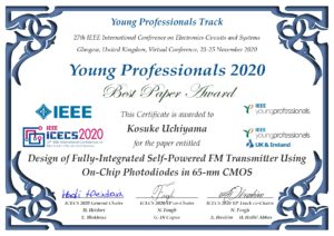
- IEEE ICECS Young Professionals 2020 Best Paper Award, Kosuke Uchiyama, Guowei CHEN and, Kiichi Niitsu, “Design of Fully-Integrated Self-Powered FM Transmitter Using On-Chip Photodiodes in 65-nm CMOS”, Nov. 2020.
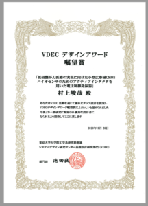
- 村上 峻哉, VDECデザインアワード嘱望賞、「低侵襲がん医療の実現に向けた小型広帯域CMOSバイオセンサのためのアクティブインダクタを用いた電圧制御発振器」2020年9月26日
- 村上 峻哉, 2020年IEEE名古屋支部国際会議研究発表賞受賞 2020年4月
- 村上 峻哉 令和元年度電気系専攻修士論文中間発表会優秀賞 2019年1月30日


Japanese Journals
- 新津 葵一、「電力自立ヘルスケア AI・IoT を実現する化学と電子情報通信技術の融合によるバイオ発電・センシングー体型集積システムの開発~単独自立動作血糖モニタリングコンタクトレンズの実現を目指して~」、化学工業7月号、化学工業社、2020年6月30日
Books and Articles
- 新津 葵一、「スマートコンタクトレンズ型グルコースセンサ」、 酵素トランスデューサーと酵素技術展開―酵素センサ&バイオ電池、そして酵素処理応用(食品,医薬,修復) CMC出版, 2020年3月11日
https://www.cmcbooks.co.jp/products/detail.php?product_id=6041 - 新津 葵一、「涙から血糖値測定、コンタクトレンズにセンサー搭載給電とセンシングを同時に行うグルコース発電素子」、コンバーテック1月号、Convertech International、加工技術研究会、2020年1月
Patents
- K.Niitsu, “Measuring device, container device, and measuring system”, No.11347083, (米国出願番号:17/052,583), (出願日:2020年11月03日) 登録
Google特許:https://patents.google.com/patent/US11347083B2/en?oq=US+11347083
(PDFダウンロード) - 新津 葵一、「測定器、収納装置および測定システム」特願2020-519885,WO2019/221166,再表2019/221166(出願日: 2019年5月15日)出願中
- 新津 葵一、 林 賢哉、 小林 敦希、 「送信装置」特願2019-062180,特開2020-162072,特許第7265756号 (出願日:2019年3月28日)登録
2019
Journals
- A. Kobayashi, K. Hayashi, S. Arata, S. Murakami, G. Xu, and K. Niitsu, “Design of a Self-Controlled Dual-Oscillator-Based Supply Voltage Monitor for Biofuel-Cell-Combined Biosensing Systems in 65-nm CMOS and 55-nm DDC CMOS”, IEEE Transactions on Biomedical Circuits and Systems (TBioCAS), vol.13, no.6, pp.1152-1162, Dec. 2019.
DOI:https://doi.org/10.1109/TBCAS.2019.2950509 - K. Hayashi, S. Arata, G. Xu, S. Murakami, C. D. Bui,A. Kobayashi and K. Niitsu, ”A 385 ×385 μm² 0.165V 0.27nW Fully-Integrated Supply-Modulated OOK Transmitterin 65nm CMOS for Glasses-Free, Self-Powered, and Fuel-Cell-Embedded Continuous Glucose Monitoring Contact Lens”, IEICE Trans. Elec.vol. E102.C no.7, pp.590-594. Jul. 2019.
DOI:https://doi.org/10.1587/transele.2018CTS0005 - K. Hayashi, S. Arata, G. Xu, S. Murakami, C. D. Bui, A. Kobayashi and K. Niitsu, ”An FSK Inductive-Coupling Transceiver Using 60mV 0.64fJ/bit 0.0016 mm² Load-Modulated transmitter and LC-Oscillator-Based Receiver in 65 nm CMOS for Energy-Budget-Unbalanced Application”, IEICE Trans. Elec. Vol.E102.C, no.7, pp.585-589. Jul. 2019.
DOI:https://doi.org/10.1587/transele.2018CTS0002 - K. Niitsu, O. Kobayashi, T. J. Yamaguchi and H. Kobayashi, ”Design and Theoretical Analysis of a Clock Jitter Reduction Circuit Using Gated Phase Blending Between Self-Delayed Clock Edges”, IEICE Electronics Express. vol. 16, no. 13, pp.20190218 Apr. 2019. DOI:https://doi.org/10.1587/elex.16.20190218
- Y. Nishio, A. Kobayashi, and K. Niitsu, ”Design and Calibration of a Small-Footprint, Low-Frequency, and Low-Power Gate Leakage Timer Using Differential Leakage Technique”, IEICE Transactions on Electronics, vol. E102.C no.4 pp.269-275, Apr. 2019.
DOI:https://doi.org/10.1587/transele.2018CDP0005 - K. Niitsu, T. Nakanishi, S. Murakami, M. Matsunaga, A. Kobayashi, N. M. Karim, J. Ito, N. Ozawa, T. Hase, H. Tanaka, M. Sato, H. Kondo, K. Ishikawa, H. Odaka, Y. Hasegawa, M. Hori, and K. Nakazato, “A 65-nm CMOS Fully-Integrated Analysis Platform Using an On-Chip Vector Network Analyzer and a Transmission-Line-Based Detection Window for Analyzing Circulating Tumor Cell and Exosome”, IEEE Transactions on Biomedical Circuits and Systems (TBioCAS), vol.13, no.2, pp.470-479, Apr. 2019.
DOI:10.1109/TBCAS.2018.2882472 - M. Matsunaga, T. Nakanishi, A. Kobayashi, K. Nakazato, and K. Niitsu, “Design and analysis of a three-dimensional millimeter-wave frequency-shift based CMOS biosensor using vertically stacked spiral inductors in LC oscillators”, Analog Integrated Circuits and Signal Processing (ALOG),vol. 98, no. 3, pp. 453-464, Mar 2019.
DOI:https://doi.org/10.1007/s10470-018-1267-5 - S. Arata, K. Hayashi, X. Ge, S. Murakami, C. D. Bui, A. Kobayashi, and K. Niitsu”Yield and open-circuit-voltage enhancement of 0.36 mm2 Solid-State CMOS-compatible glucose fuel cell by using repeated separator coating”, Japanese Journal of Applied Physics, vol.58, no.SB, pp.SBBG11, Feb. 2019.
DOI:https://doi.org/10.7567/1347-4065/aafc9e
International Conferences
- S. Murakami, T. Nakanishi, A. Kobayashi, M. Z.Islam, and K. Niitsu, “LC-Voltage-Controlled-Oscillator-Based Biosensor in 180-nm CMOS Process Targeting β-Dispersion for Detecting Exosomes”, in Proc. 2019 IEEE Asia Pacific Conference on Circuits and Systems (APCCAS)
DOI:10.1109/APCCAS47518.2019.8953109 - A. Kobayashi, K. Hayashi, S. Arata, G. Xu, S. Murakami, C. D. Bui, T. M. Quan, M. Z. Islam, K. Niitsu “A Solar-Cell-Assisted, 99.66% Biofuel Cell Area Reduced, Biofuel-Cell-Powered Wireless Biosensing System in 65-nm CMOS for Continuous Glucose Monitoring Contact Lenses”, in Proc. 2019 26th IEEE International Conference on Electronics, Circuits and Systems (ICECS).
DOI:10.1109/ICECS46596.2019.8965102 - S. Murakami, T. Nakanishi, A. Kobayashi, M. Z. Islam, K. Niitsu “Verification of Inductive-Coupling-Based CMOS Biosensor Focusing Dielectric Loss of β-Dispersion for Detecting Exosomes Through Electromagnetic Simulation”, in Proc. IEEE International Conference on Electronics, Circuits and Systems (ICECS 2019).
DOI:10.1109/ICECS46596.2019.8964844 - T. Nakanishi, S. Murakami, A. Kobayashi, M. Z. Islam, and K. Niitsu “A 40-GHz Fully-Integrated CMOS-Based Biosensor Circuit With an On-Chip Vector Network Analyzer for Circulaitng Tumor Cells Analysis”, in proc. 2019 IEEE Nordic Circuits and Systems Conference (NORCAS): NORCHIP and International Symposium of System-on-Chip (SoC)
DOI: 10.1109/NORCHIP.2019.8906936 - A. Kobayashi, K. Hayashi, S. Arata, S. Murakami, G. Xu, M. Z. Islam, and K. Niitsu, “A 2.1-nW Burst-Pulse-Counting Supply Voltage Monitor for Biofuel-Cell-Combined Biosensing Systems in 180-nm CMOS”, in Proc. 2019 IEEE Biomedical Circuits and Systems Conference (BioCAS)
DOI:10.1109/BIOCAS.2019.8918978 - M. Z. Islam, S. Arata, K. Hayashi, A. Kobayashi, Y. Momoi and K. Niitsu, “1D structural CNH dependency in needle type Solid-state CMOS compatible glu-cose Fuel Cell for open-circuit voltage and their biomedical application”, in Proc. 2019 international Conference on Solid State Devices and Materials, Sep.2019.
- S. Murakami, T. Nakanishi, A. Kobayashi, M. Z. Islam, K. Niitsu, “Design of Inductive-Coupling-Based CMOS Biosensor Focusing Dielectric Loss of βDispersion for Detecting Exosomes”, in proc. 2019 Taiwan and Japan Conference on Circuits and Systems (TJCAS 2019 at Nikko), Aug. 2019.
- T. Nakanishi, S. Murakami, A. Kobayashi, Md. Z. Islam, K. Niitsu, “A 40-GHz Fully Integrated On-Chip-VNA-based Circulating Tumor Cells Analyzer in 65-nm CMOS Technology”, in proc. 2019 Taiwan and Japan Conference on Circuits and Systems (TJCAS 2019 at Nikko), Aug. 2019.
- K. Uchiyama, S. Jodo, S. Murakami, M. Z. Islam, A. Kobayashi, K. Niitsu,”Design of On-Chip Integrated Solar Cells in 65nm CMOS Technology for Solar-Cell-Powered Continuous Glucose Monitoring Systems”, in proc. 2019 Taiwan and Japan Conference on Circuits and Systems (TJCAS 2019 at Nikko), Aug. 2019.
- S. Jodo, C. D. Bui, K. Uchiyama, M. Z. Islam, A. Kobayashi, K. Niitsu,”Design of CMOS GaN Gate Driver for 13.56MHz GaN-Based Power Electronics Application in 180nm High-Voltage CMOS Technology”, in proc. 2019 Taiwan and Japan Conference on Circuits and Systems (TJCAS 2019 at Nikko), Aug. 2019.
- R. Sakai, S. Murakami, T. Nakanishi, M. Z. Islam, A. Kobayashi, K. Niitsu,”Desing of A CML-Based NMOS-Only SelfOscillating Voltage Doubler for Enabling UltraLow Start-Up Voltage in 65-nm CMOS Technology”, in proc. 2019 Taiwan and Japan Conference on Circuits and Systems (TJCAS 2019 at Nikko), Aug. 2019.
- M. Z. Islam, S. Arata, K. Hayashi, A. Kobayashi, Y. Momoi and K. Niitsu, ”Enhance OCV of CNH dependency in Solid-state CMOS compatible glucose Fuel Cell for next-generation internet of things (IoT)”, in Proc. Molecular Electronics and Bioelectronics (M&BE), Jun. 2019.
- K. Hayashi, S. Arata, G. Xu, S. Murakami, C. D. Bui, A. Kobayashi, and K. Niitsu,”0.27nW Fully-Integrated Supply-Modulated OOK Transmitter in 65nm CMOS for Self-Powered and Low-Cost Continuous Glucose Monitoring Contact Lens”, in Proc. 11th International Symposium on Advanced Plasma Science and its Applications for Nitrides and Nano materials / 12th International Conference on Plasma-Nano Technology & Science (ISPlasma2019 / IC-PLANTS2019), p.832, Mar. 2019.
- M. Z. Islam, S. Arata, K. Hayashi, A. Kobayashi and K. Niitsu,”Various Type of CNT Dispersion Applied to Bio-Fuel Cell for High Yield of Production”, in Proc. 11th International Symposium on Advanced Plasma Science and its Applications for Nitrides and Nano materials / 12th International Conference on Plasma-Nano Technology & Science (ISPlasma2019 / IC-PLANTS2019), p.8323, Mar. 2019.
- A. Kobayashi, K. Hayashi, S. Arata, S. Murakami, G. Xu, and K. Niitsu“A 65-nm CMOS 1.4-nW Self-Controlled Dual-Oscillator-Based Supply Voltage Monitor for Biofuel-Cell-Combined Biosensing Systems”,2019 IEEE International Symposium on Circuits and Systems (ISCAS)
DOI:10.1109/ISCAS.2019.8702693 - T. M. Quan, T. Doike, D. C. Bui, K. hayashi, S. Arata, A. Kobayashi, Md. Z. Islam, K. Niitsu, “AI-Based Edge-Intelligent Hypoglycemia Prediction System Using Alternate Learning and Inference Method for Blood Glucose Level Data with Low-periodicity”, in 2019 IEEE International Conference on Artificial Intelligence Circuits and Systems (AICAS)
DOI: 10.1109/AICAS.2019.8771604 - T. Nakanishi, M. mmMatsunaga, S. Murakami, A. Kobayashi, K. Niitsu, “A 65-nm CMOS Fully-Integrated Circulating Tumor Cell and Exosome Analyzer Using an On-Chip Vector Network Analyzer and a Transmission-Line-Based Detection Window”, in Proc. IEEE/ACM Proc. ACM/IEEE Asia and South Pacific Design Automation Conference (ASP-DAC 2019), Jan. 2019. DOI: https://doi.org/10.1145/3287624.3287750
- K. Niitsu, Y. Yamaji, A. Kobayashi, K. Nakazato”A Low-Voltage CMOS Electrophoresis IC Using Electroless Gold Plating for Small-Form-Factor Biomolecule Manipulation”, in Proc. IEEE/ACM Proc. ACM/IEEE Asia and South Pacific Design Automation Conference (ASP-DAC 2019), Jan. 2019. DOI: https://doi.org/10.1145/3287624.3287755
- A. Kobayashi, Y. Nishio, K. Hayashi, S. Arata, K. Niitsu “Design of Gate-Leakage-Based Timer Using an Amplifier-Less Replica-Bias Switching Technique in 55-nm DDC CMOS”, in Proc. IEEE/ACM Proc. ACM/IEEE Asia and South Pacific Design Automation Conference (ASP-DAC 2019), Jan. 2019. DOI: https://doi.org/10.1145/3287624.3287756
- K. Niitsu, T. Sakabe, M. Miyachi, Y. Yamanoi, H. Nishihara, T. Tomo, K. Nakazato, “2D Optical Imaging Using Photosystem I Photosensor Platform with 32×32 CMOS Biosensor Array”, in Proc. IEEE/ACM Proc. ACM/IEEE Asia and South Pacific Design Automation Conference (ASP-DAC 2019), Jan. 2019. DOI: https://doi.org/10.1145/3287624.3287751
- K. Hayashi, S. Arata, G. Xu, S. Murakami, C. D. Bui, T. Doike, M. Matsunaga, A. Kobayashi, K. Niitsu,”Design of 385 x 385 µm2 0.165V 270pW Fully-Integrated Supply-Modulated OOK Transmitter in 65nm CMOS for Glasses-Free, Self-Powered, and Fuel-Cell-Embedded Continuous Glucose Monitoring Contact Lens”, in Proc. IEEE/ACM Proc. ACM/IEEE Asia and South Pacific Design Automation Conference (ASP-DAC 2019), Jan. 2019.
DOI: https://doi.org/10.1145/3287624.3287753 - M. Matsunaga, T. Nakanishi, A. Kobayashi, K. Niitsu, “A Three-Dimensional Millimeter-Wave Frequency-Shift Based CMOS Biosensor using Vertically Stacked Spiral Inductors in LC Oscillators”, in Proc. IEEE/ACM Proc. ACM/IEEE Asia and South Pacific Design Automation Conference (ASP-DAC 2019), Jan. 2019.
DOI: https://doi.org/10.1145/3287624.3287749
Invited Talks
- [Plenary] K. Niitsu, ”Energy-Autonomous AI/IoT Platform for Unconscious Healthcare ~Stand-Alone Continuous Glucose Monitoring Smart Contact Lenses~”,30th 2019 International Symposium on Micro-NanoMechatronics and Human Science, Dec. 2019. (Nagoya, Japan)
- 新津 葵一、「AI(人工知能)とIoT(モノのインターネット)によって変革する未来の”無意識な”医療とヘルスケア~世界初の単独自立動作可能エッジAI機能付き持続血糖モニタリングコンタクトレンズの開発を通じて~」、あいちサイエンスフェスティバル2019@鶴舞中央図書館 「図書館サイエンス夜話」、2019年11月21日(愛知県)
- 新津 葵一、「小型生物ナビゲーションに向けた発電センシング一体型集積血糖センサ技術の開発」、第37回日本ロボット学会学術講演会、2019年9月7日(東京都)
- 新津 葵一、「AIとIoTの連携による未来の医療・ヘルスケア~単独動作可能持続血糖モニタリングコンタクトレンズ~」、センシング技術コンソーシアム第28回講演会、2019年9月2日(愛知県)
- 新津 葵一、「生体情報センシングに向けたフレキシブルデバイス技術動向と今後の展望」、新化学技術推進協会次世代エレクトロニクス分科会講演会、2019年8月7日(東京都)
- 新津 葵一、「AIとIoTが切り開く未来の医療・ヘルスケア ~単独動作可能エッジAI機能付き持続血糖モニタリングコンタクトレンズの研究開発を通して~」、関西コンバーティングモノづくり研究会、2019年4月12日(大阪府)
- 新津 葵一、「ナノテク応用サブナノワット集積ヘルスケアIoT ~単独動作可能・電力自立持続血糖モニタリングコンタクト~」、第17回ナノテクノロジー総合シンポジウム 2019年2月1日(東京都)
- [Plenary] K. Niitsu, ”CMOS biomedical IoT design for tissue engineering and regenerative medicine”, The 3rd Conference on Tissue Engineering and Regenerative Medicine (CTERM 2019) , Jan. 2019. (中国・三亜)
Awards
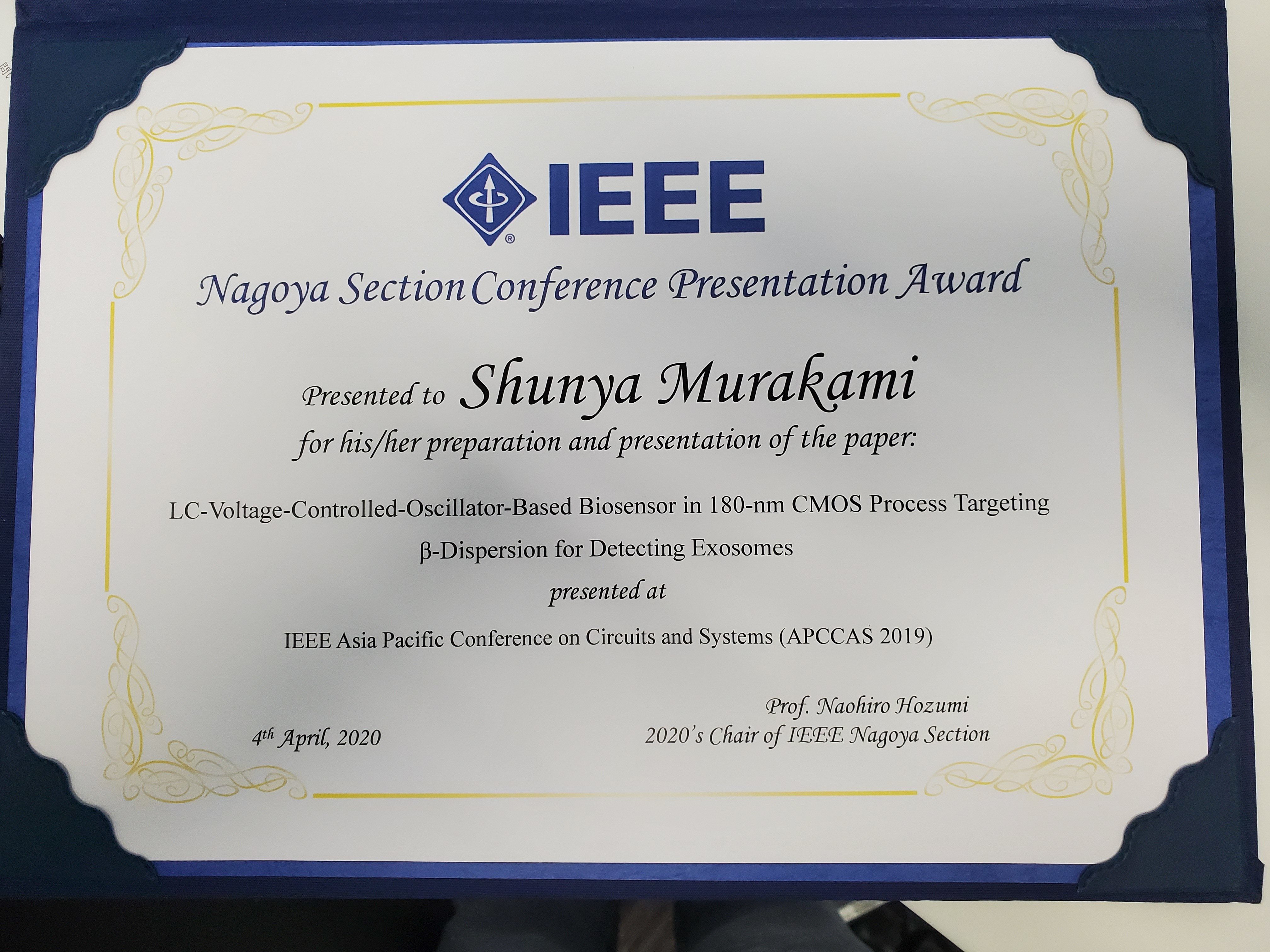
- 新津 葵一、「発電センシング一体型集積センサ技術を用いた単独動作可能・電力自立持続血糖モニタリングコンタクトレンズの研究開発」、第3回「バイオインダストリー奨励賞」(一般財団法人 バイオインダストリー協会)、2019年10月9日 https://www.jba.or.jp/jba/osirase/3_3.php
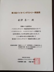
- 林 賢哉,荒田 滋樹,小林 敦希,新津 葵一、「単独動作可能な血糖モニタリングシステムに向けたグルコース発電素子と65nm COMS 0.165V 0.27nW 無線送信回路による電力自立・低コストバイオセンサ集積回路」、IEEE SSCS Kansai Chapter Academic Research Award,2019年5月14日
- 林 賢哉 平成30年度電気系専攻修士論文中間発表会優秀賞 2019年1月24日 修士論文中間発表優秀賞_林賢哉
- M. Matsunaga, T. Nakanishi, A. Kobayashi, K. Niitsu, IEEE/ACM (ASP-DAC) 2019 Special Feature Award, “A Three-Dimensional Millimeter-Wave Frequency-Shift Based CMOS Biosensor using Vertically Stacked Spiral Inductors in LC Oscillators,” Jan. 22, 2019.
- K.Hayashi, S. Arata, G. Xu, S. Murakami, C. D. Bui, T. Doike, M. Matsunaga, A. Kobayashi, Kiichi Niitsu ,IEEE/ACM (ASP-DAC) 2019 Special Feature Award, “Design of 385 x 385 µm2 0.165V 270pW Fully-Integrated Supply-Modulated OOK Transmitter in 65nm CMOS for Glasses-Free, Self-Powered, and Fuel-Cell-Embedded Continuous Glucose Monitoring Contact Lens,” Jan. 22, 2019.
- K. Hayashi 論文 A Three-Dimensional Millimeter-Wave Frequency-Shift Based CMOS Biosensor using Vertically Stacked Spiral Inductors in LC Oscillators 2019年
Patents
- 新津 葵一, 林 賢哉, 小林 敦希, 「高信頼・低消費電力・電波有効利用バイオメディカルIoTの実現に向けたパッシブ型人体通信技術の開発」(出願日:2019年3月)
- 新津 葵一、西尾 祐哉、林 賢哉、小林 敦希、「集積回路用低周波数信号発生回路素子」特願2018-074251,特開2019-186711,特許第7042486号(出願日:2018年4月6日)登録
Press Release
- 「針刺さずに血糖値測定 糖尿病予防に期待 名古屋大学など センサー開発」日本経済新聞、 2019年6月18日
(PDFダウンロード) - 「名古屋大の研究チームが「30分後の低血糖」を予測するシステムを開発」Med It Tech、2019年4月17日
(PDFダウンロード) - 「人工知能(AI)を使った血糖値予測システムを開発 30分後の血糖値を予測」日本生活習慣病予防協会、2019年4月15日
(PDFダウンロード) - 「人工知能(AI)を使った血糖値予測システムを開発 30分後の血糖値を予測」糖尿病ネットワーク、2019年4月12日
(PDFダウンロード) - 「名大,AIによる血糖値予測システムを開発」OPTRONICS ONLINE、2019年04月9日
(PDFダウンロード) - 「人工知能を用いた血糖値予測システムを新たに開発-名大」QlifePro、2019年4月9日
(PDFダウンロード)
Visiting Lecture
- 愛知県立一宮西高等学校、「大学説明会及び模擬授業」2019年7月2日
2018
Journals
- K. Hayashi, S. Arata, S. Murakami, Y. Nishio, A. Kobayashi, and K. Niitsu, “A 6.1nA Fully-Integrated CMOS Supply-Modulated OOK Transmitter in 55nm DDC CMOS for Glass-Free, Self-Powered, and Fuel-Cell-Embedded Continuous Glucose Monitoring Contact Lens“, IEEE Transactions on Circuits and Systems II (TCAS-II). vol.65, no.10, pp.1360-1364, Oct. 2018.
DOI:10.1109/TCSII.2018.2860636 - K. Niitsu, ”Energy-Autonomous Biosensing Platform Using Supply-Sensing CMOS Integrated Sensor and Bio Fuel Cell for Next-Generation Healthcare Internet of Things”, Japanese Journal of Applied Physics. vol.57, no.10, pp.1002A5, Sep. 2018.
DOI:https://doi.org/10.7567/JJAP.57.1002A5 - K. Niitsu, A. Kobayashi, K. Hayashi, Y. Nishio, K. Ikeda, T. Ando, Y. Ogawa, H. Kai, M. Nishizawa, and K. Nakazato, “A Self-Powered Supply-Sensing Biosensor Platform Using Bio Fuel Cell and Low-Voltage, Low-Cost CMOS Supply-Controlled Ring Oscillator with Inductive-Coupling Transmitter for Healthcare IoT,” IEEE Transactions on Circuits and Systems I (TCAS-I).vol.65, no.9, pp.2784-2796, Sep. 2018.
DOI:10.1109/TCSI.2018.2791516 - S. Arata, K. Hayashi, Y. Nishio, A. Kobayashi, K. Nakazato, and K. Niitsu, “Wafer-scale development and experimental verification of 0.36-mm^2 228-mV open-circuit-voltage solid-state CMOS-compatible glucose fuel cell for healthcare IoT application,” Japanese Journal of Applied Physics. vol.57, no.4S, pp.04FM04, Mar. 2018.
DOI:https://doi.org/10.7567/JJAP.57.04FM04 - M. Matsunaga, A. Kobayashi, K. Nakazato, and K. Niitsu, “Design Trade-Off between Spatial Resolution and Power Consumption in CMOS Biosensor Circuit Based on Millimeter-Wave LC-Oscillator Array,” Japanese Journal of Applied Physics, vol. 57, no. 3S2, pp. 03EC02, Jan. 2018.
DOI:https://doi.org/10.7567/JJAP.57.03EC02 - T. Nakanishi, M. Matsunaga, A. Kobayashi, K. Nakazato, and K. Niitsu, “A 40-GHz fully integrated circulating tumor cell analysis vector network analyzer in 65-nm CMOS technology with coplanar-line-based detection area,” Japanese Journal of Applied Physics, vol. 57, no. 3S2, pp. 03EC01, Jan. 2018.
DOI:https://doi.org/10.7567/JJAP.57.03EC01 - K. Itakura, K. Kayano, K. Nakazato and K. Niitsu, “Theoretical Analysis and Simulation Study of Low-Power CMOS Electrochemical Impedance Spectroscopy Biosensor in 55nm DDC Technology for Cell-State Monitoring,” Japanese Journal of Applied Physics, vol. 57, no. 1S, pp. 01AG02, Jan. 2018.
DOI:https://doi.org/10.7567/JJAP.57.01AG02
International Conferences
- S. Arata, K. Hayashi, X. Ge, S. Murakami, C. D. Bui, A. Kobayashi, and K. Niitsu, “Reactive Ion Etching in Development of 0.6mm by 0.6mm CMOS-Compatible Solid-State Glucose Fuel Cell for Small-Form-Factor Biomedical IoT Applications,” in Proc. International Symposium on Dry Process (DPS 2018), p. 1, Nov. 2018.
- K. Liu, Y. Min, X. Yang, H. Sun and H. Shinohara, “A 373 F2 2D Power-Gated EE SRAM Physically Unclonable Function With Dark-Bit Detection Technique”, 2018 IEEE Asian Solid-State Circuits Conference (A-SSCC), Nov. 2018.
DOI: 10.1109/ASSCC.2018.8579315 - S. Murakami, K. Hayashi, S. Arata, G. Xu, C. D. Bui, A. Kobayashi and K. Niitsu, Affiliation “A Stochastic Oscillator Using Multiple Ring Oscillators and OR-Gate for Low Voltage Operation in 65 nm CMOS,”in Proc. IEEE Asia Pacific Conference on Postgraduate Research in Microelectronics and Electronics(PrimeAsia 2018), China, Oct. 2018.
DOI: 10.1109/PRIMEASIA.2018.8597600 - K. Kayano, M. Matsunaga, K. Itakura, A. Kobayashi and K. Niitsu, “Design of an Energy-Autonomous Supply-Sensing Biosensor Platform Using Biofuel Cells and Human-Body-Communication Transmitter,” in Proc. EEE Asia Pacific Conference on Postgraduate Research in Microelectronics and Electronics(PrimeAsia 2018), China, Oct. 2018.
DOI: 10.1109/PRIMEASIA.2018.8597942 - Y. Nishio, A. Kobayashi and K. Niitsu, “A Constant-Power Inductive-Coupling Transmitter Using Auxiliary Driving Technique in 65nm SOTB CMOS for Low-Power Supply-Sensing Biosensing Platform toward Healthcare IoTs,” in Proc. IEEE Asia Pacific Conference on Circuits and Systems (APCCAS 2018), pp. 1-4, Oct. 2018.
DOI:10.1109/APCCAS.2018.8605645 - G. Xu, K. Hayashi, S. Arata, S. Murakami, C. D. Bui, A. Kobayashi and K. Niitsu, “A BER-Modulated 3-Coil Inductive-Coupling Transceiver Using Dynamic Intermediate Interference Control Technique,” in Proc. IEEE Asia Pacific Conference on Circuits and Systems (APCCAS 2018), pp. 1-4, Oct. 2018.
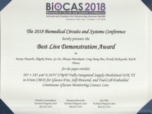
DOI: 10.1109/APCCAS.2018.8605709 - K. Hayashi, S. Arata, G. Xu, S. Murakami, D. C. Bui, T, Doike, M. Matsunaga, A. Kobayashi, and K. Niitsu, “Live Demonstration: 385 X 385 µm2 0.165V 270pW Fully-Integrated Supply-Modulated OOK TX in 65nm CMOS for Glasses-Free, Self-Powered, and Fuel-Cell-Embedded Continuous Glucose Monitoring Contact Lens,” in Proc. IEEE Biomedical Circuits and Systems Conference (BioCAS 2018), p. 1, Oct. 2018.
DOI:https://doi.org/10.1109/BIOCAS.2018.8584841 - S. Arata, K. Hayashi, X. Ge, S. Murakami, D. C. Bui, A. Kobayashi, and K. Niitsu, “10% Yield and 370-mV OCV of 0.36 mm2 Solid-State CMOS-Compatible Glucose Fuel Cell by Using Repeated Separator Coating,” in Proc. International Conference on Solid State Devices and Materials (SSDM 2018), Sep. 2018.
- K. Hayashi, S. Arata, S. Murakami, Y. Nishio, A. Kobayashi, and K. Niitsu, “A 6.1nA Fully-Integrated CMOS Supply-Modulated OOK Transmitter in 55nm DDC CMOS for Glass-Free, Self-Powered, and Fuel-Cell-Embedded Continuous Glucose Monitoring Contact Lens”, in Proc. IEEE The International Symposium on Integrated Circuits and Systems (ISICAS), Sep. 2018. (Taormina, Italy)
DOI: 10.1109/TCSII.2018.2860636 - T. Doike, K. Hayashi, S. Arata, K. N. Mohammad, A. Kobayashi, and K. Niitsu, “A Blood Glucose Level Prediction System Using Machine Learning Based on Recurrent Neural Network for Hypoglycemia Prevention,” in Proc. IEEE International NEWCAS Conference 2018 (NEWCAS 2018), Jun. 2018. DOI: 10.1109/NEWCAS.2018.8585468
- K. Niitsu, T. Sakabe, M. Miyachi, Y. Yamanoi, H. Nishihara, T. Tomo, K. Nakazato, “Demonstration of 2D Optical Imaging Using Photosystem I Photosensor Platform with 32×32 CMOS Biosensor Array,” in Proc. IEEE International NEWCAS Conference 2018 (NEWCAS 2018), Jun. 2018. DOI: 10.1109/NEWCAS.2018.8585603
- A. Kobayashi, Y. Nishio, K. Hayashi, K. Nakazato, and K. Niitsu, “A 350-mV, Under-200-ppm Allan Deviation Floor Gate-Leakage-Based Timer Using an Amplifier-Less Replica-Bias Switching Technique in 55-nm DDC CMOS,” in Proc. IEEE Custom Integrated Circuit Conference (CICC 2018), pp.1-4, Apr. 2018.
DOI: 10.1109/CICC.2018.8357093 - R. Zhang, S. Chen, C. Wan and H. Shinohara, “High-throughput Von Neumann post-processing for random number generator”, 2018 International Symposium on VLSI Design, Automation and Test (VLSI-DAT), Apr. 2018.
DOI: 10.1109/VLSI-DAT.2018.8373253 - T. Doike and K. Niitsu, “An AI-Enhanced Blood Glucose Sensing System Using Machine Learning Based on Recurrent Neural Network for Hypoglycemia Prevention,” Proc. 10th International Symposium on Advanced Plasma Science and its Applications for Nitrides and Nano materials / 11th International Conference on Plasma-Nano Technology & Science (ISPlasma2018 / IC-PLANTS2018), pp. 07P65, Mar. 2018.
- S. Nagata, N. Kameshiro, D. Terutsuki, H. Mitsuno, T. Sakurai, K. Niitsu, K. Nakazato, R. Kanzaki, and M. Ando, “A HIGH-DENSITY INTEGRATED ODORANT SENSOR ARRAY SYSTEM BASED ON INSECT CELLS EXPRESSING INSECT ODORANT RECEPTORS,” in Proc. IEEE International Conference on Micro Electro Mechanical Systems (MEMS 2018), Jan. 2018.
DOI: 10.1109/MEMSYS.2018.8346540
Invited Talks
- 新津 葵一、「Society5.0時代のスマート社会・スマートライフ実現に資するバイオ燃料電池を用いた電力自立継続血糖バイオセンサ技術」、第28回 日本MRS年次大会 B-5 : スマート社会・スマートライフのためのバイオセンサ・バイオ燃料電池、2018年12月 (北九州市)
- 新津 葵一、「医療ビッグデータ連携ヘルスケアに向けた使い捨て可能・電力自立バイオセンサ集積回路技術の開発」、ICTイノベーションフォーラム2018、2018年10月10日 (東京都)
- [Tutorial] Kiichi Niitsu, “Self-Powered and Energy-Autonomous CMOS biomedical IoT design for personalized health care systems”, IEEE Asia Pacific Conference on Circuits and Systems (APCCAS 2018), Oct. 2018.(中国・成都)
- [Invited] Kiichi Niitsu, “An Energy-Autonomous Biomedical IoT Platform Using Human Computer Ion-Coupled Energy Interaction for Next-Generation Diabetes Care”, International Conference on Solid-State Devices and Materials (SSDM), Sep. 2018.(東京都)
- [Tutorial] K. Niitsu, “Introduction of CMOS Biosensor Design for Biomedical IoT Applications,” IEEE NEWCAS Conference (NEWCAS 2018), Jun. 2018.(カナダ・モントリオール)
- 新津 葵一、「低消費電力CMOS集積回路システムとバイオ発電素子を用いた電力自立発電センシング一体型集積血糖センサによる糖尿病医療・予防革新~ヘルスケアIoT開発国プロ成果の社会実装に向けて~」、電子情報通信学会総合大会、メディカル応用に向けた回路とシステム、2018年3月23日 (東京都)
- [Invited] K. Niitsu, ” Energy-Autonomous Supply-Sensing Biosensor Using Low-Power CMOS LSI and Biofuel Cell for Low-invasive Edge-intelligent Blood Glucose Monitoring” in Proc. The 6th Asian Workshop on Smart Sensor System (AWSSS 2018), Mar. 2018. (台湾・桃園)
- [Invited] K. Niitsu, “Biomedical IoTs Using Plasma-Enhanced CMOS Electronics -From Low-Cost Small-Form-Factor CTC/Exosome Analysis for Liquid Biopsy to Energy-Autonomous Continuous Glucose Monitoring Platform-,” International workshop on plasma synthesis of nanomaterials and its applications for sensor devices, Mar. 2018. (岐阜県郡上市)
- [Invited] K. Niitsu, “Energy-autonomous Biomedical IoTs using Plasma-enhanced Bio-fuel Cell and Low-energy CMOS Biosensor,” in Proc. 10th International Symposium on Advanced Plasma Science and its Applications for Nitrides and Nano materials / 11th International Conference on Plasma-Nano Technology & Science (ISPlasma2018 / IC-PLANTS2018), pp. 06pA14I, Mar. 2018. (名古屋市)
Awards
- K. Hayashi, S. Arata, G. Xu, S. Murakami, D. C. Bui, T. Doike, M. Matsunaga, A. Kobayashi, and K. Niitsu, IEEE Biomedical Circuits and Systems Conference (BioCAS) 2018 Best Live Demonstration Award (IEEE) 2018年10月18日
- 新津 葵一, 電子情報通信学会 末松安晴賞, 「低電圧・低消費電力時間分解能型CMOS集積回路技術の開拓とその医療応用への展開」, 2018年6月7日
- 中西 大貴、松永 摩耶、小林 敦希、中里 和郎、新津 葵一, CST YEP Award 2017 特別賞, 2018年3月
- 小林 敦希, IEEE名古屋支部優秀学生賞, 2018年3月26日
Press Release
- 「コンタクトレンズを装着するだけで血糖値を持続的にモニタリング」糖尿病ネットワーク 2018年10月25日
(PDFダウンロード) - 「血糖をモニタリングするコンタクトレンズ型装置の試作に名古屋大学が成功」大学ジャーナルオンライン 2018年10月28日
(PDFダウンロード) - 「コンタクトレンズを装着するだけで血糖値を持続的にモニタリング 無線給電が不要の世界最小センサーを開発 名古屋大学」糖尿病リソースガイド 2018年10月23日
(PDFダウンロード) - 「給電端末が不要なコンタクトレンズ方式の持続型血糖モニタリング装置を試作-名大」医療NEWS 2018年10月22日
(PDFダウンロード) - 「血糖値コンタクトで測定 名大 実用化目指す」朝日新聞朝刊 2018年10月18日
- 「コンタクトにつけて血糖値測定 超小型の装置開発」朝日新聞デジタル 2018年10月17日
- 「名大とJST、世界最小クラスの発電・センシング一体型血糖センサーを開発-コンタクトレンズ方式の血糖管理を実現へ」日本経済新聞、2018年10月17日
(PDFダウンロード)
Books and Articles
- K. Niitsu, “Energy-autonomous biosensing platform using supply-sensing CMOS integrated sensor and biofuel cell for next-generation healthcare Internet of Things”, Japanese Journal of Applied Physics:SELECTED TOPICS IN APPLIED PHYSICS, vol.57, no.10, pp.1002A5, Sep. 2018.
https://doi.org/10.7567/JJAP.57.1002A5 - 新津 葵一、「CMOS集積回路技術を用いたバイオセンサ集積システム」、電子情報通信学会 Fundamentals Review、12巻、133-143頁、2018年
Patents
- 新津 葵一、 牛島 栄造、 岩田 裕司、中里 和郎、「生体分子検出装置および生体分子検出装置の製造方法」特願2016-172865,特開2018-040580,特許第6759881号(出願日:2016年9月5日)登録
Academic Societies
- IEEE International Conference on Electronics, Circuits and Systems 2018 (ICECS 2018) Technical Program Committee Member (2018年度)
- 第35回センサシンポジウム実行委員 (2018年度~現在)
- 応用物理学会 応用物理学会東海地区若手チャプター コアメンバー (2018年1月~現在)
2017
Journals
- A. Kobayashi, K. Ikeda, Y. Ogawa, H. Kai, M. Nishizawa, K. Nakazato, and K. Niitsu, “Design and Experimental Verification of 0.19 V 53 μW 65 nm CMOS Integrated Supply-Sensing Sensor with a Supply-Insensitive Temperature Sensor and Inductive-Coupling Transmitter for a Self-Powered Bio-Sensing Using a Biofuel Cell”, IEEE Transactions on Biomedical Circuits and Systems (TBioCAS), vol. 11, no. 6, pp. 1313-1323, Dec. 2017.
DOI: https://doi.org/10.1109/TBCAS.2017.2735447 - K. Ikeda, A. Kobayashi, K. Nakazato, and K. Niitsu, “Design and Electrochemical Measurement of a Current-Mode Analog-to-Time Converter with Short-Pulse Output Capability Using Local Intra-Cell Activation for High-Speed Time-Domain Biosensor Array”, Analog Integrated Circuits and Signal Processing (ALOG), vol. 92, no. 3, pp. 403-413, Jun. 2017.
DOI: https://doi.org/10.1007/s10470-017-1003-6 - K. Ikeda, A. Kobayashi, K. Nakazato, and K. Niitsu, “Design and Analysis of Scalability in Current-Mode Analog-to-Time Converter for an Energy-Efficient and High-Resolution CMOS Biosensor Array”, IEICE Transactions on Electronics, vol. E100-C, no. 6, pp. 597-601, Jun. 2017.
DOI: https://doi.org/10.1587/transele.E100.C.597 - K. Gamo, K. Nakazato, and K. Niitsu, “A Current-Integration-Based CMOS Amperometric Sensor with 1024 × 1024 Bacteria-Sized Microelectrode Array for High-Sensitivity Bacteria Counting”, IEICE Transactions on Electronics, vol.E100-C, no. 6, pp. 602-606, Jun. 2017.
DOI: https://doi.org/10.1587/transele.E100.C.602 - Y. Yamaji, K. Nakazato, and K. Niitsu, “Sub-1-V CMOS-Based Electrophoresis Using Electroless Gold Plating for Small-Form-Factor Biomolecule Manipulation”, IEICE Transactions on Electronics, vol. E100-C, no. 6, pp. 592-596, Jun. 2017.
DOI: https://doi.org/10.1587/transele.E100.C.592 - A. Kobayashi, K. Ikeda, K. Nakazato, and K. Niitsu, “Energy-efficient and low-voltage design methodology for a supply-sensing CMOS biosensor using biofuel cells for energy-autonomous healthcare applications”, Japanese Journal of Applied Physics, vol. 56, no. 1S, pp. 01AH03, Jan. 2017.
DOI:https://doi.org/10.7567/JJAP.56.01AH0 - K. Niitsu, T. Ando, and K. Nakazato, “Enhancement in open-circuit voltage of implantable CMOS-compatible glucose fuel cell by improving the anodic catalyst”, Japanese Journal of Applied Physics, vol. 56, no. 1S, pp. 01AH04, Jan. 2017.
DOI:https://doi.org/10.7567/JJAP.56.01AH04 - K. Niitsu, A. Kobayashi, K. Yoshida, and K. Nakazato, “Design and experimental verification of CMOS Magnetic-Based Microbeads Detection Using an Asynchronous Intra-chip Inductive-Coupling Transceiver”, Japanese Journal of Applied Physics, vol. 56, no. 1S, pp. 01AH05, Jan. 2017.
DOI:https://doi.org/10.7567/JJAP.56.01AH05 - K. Gamo, K. Nakazato, and K. Niitsu, “Design, theoretical analysis, and experimental verification of a CMOS current integrator with 1.2 × 2.05 µm2 microelectrode array for high-sensitivity bacterial counting”, Japanese Journal of Applied Physics, vol. 56, no. 1S, pp. 01AH01, Jan. 2017
DOI:https://doi.org/10.7567/JJAP.56.01AH01 - K. Niitsu, K. Ikeda, K. Muto, and K. Nakazato, “Design, Experimental Verification, and Analysis of a 1.8-V-Input-range Voltage-to-Current Converter Using Source Degeneration for Low-Noise Multimodal CMOS Biosensor Array”, Japanese Journal of Applied Physics, vol. 56, no. 1S, pp. 01AH06, Jan. 2017.
DOI:https://doi.org/10.7567/JJAP.56.01AH06
International Conferences
- Y. Nishio, A. Kobayashi, and K. Niitsu, “A 28um 2, 0.11Hz, 4.5pW Gate Leakage Timer Using Differential Leakage Technique in 55nm DDC CMOS for Small-Footprint, Low-Frequency and Low-Power Timing Generation,” in Proc. IEEE International Conference on Electronics, Circuits and Systems (ICECS 2017), pp. 1-4, Dec. 2017.
DOI: 10.1109/ICECS.2017.8292063 - K. Ikeda, A. Kobayashi, and K. Niitsu, “A Scalable Time-Domain Biosensor Array Using a Capacitor-Less CMATC and Logarithmic Cyclic Time-Attenuation-Based TDC with Discharge Acceleration for High-Spatial-Resolution Bio-Imaging,” in Proc. IEEE International Conference on Electronics, Circuits and Systems (ICECS 2017), pp. 1-4, Dec. 2017.
DOI: 10.1109/ICECS.2017.8292072 - M. Matsunaga, T. Nakanishi, A. Kobayashi, K. Nakazato, and K. Niitsu, “Three-Dimensional Millimeter-wave Frequency-shift-based CMOS Biosensor Using Vertically Stacked LC Oscillators,” in Proc. IEEE Nordic Circuits and Systems Conference (NorCAS 2017), pp. 1-6, Oct. 2017. DOI: 10.1109/NORCHIP.2017.8124974.
- T. Nakanishi, M. Matsunaga, A. Kobayashi, K. Nakazato and K. Niitsu, “A Fully-Integrated Circulating Tumor Cell Analyzer Using an on-Chip Vector Network Analyzer and a Transmission-Line-Based Detection Window in 65-nm CMOS,” in Proc. IEEE Biomedical Circuits and Systems Conference (BioCAS 2017), pp. 1-4, Oct. 2017.
DOI: 10.1109/BIOCAS.2017.8325554 - E. Ushijima, S. Fujimoto, K. Niitsu, and K. Nakazato, “Application of Magnetic Arrangement of Microbeads for CMOS Biosensor Array Sensitivity,” in Proc. IEEE Biomedical Circuits and Systems Conference (BioCAS 2017), pp. 1-4, Oct. 2017.
DOI: 10.1109/BIOCAS.2017.8325048 - S. Arata, K. Hayashi, Y. Nishio, A. Kobayashi, K. Nakazato, and K. Niitsu, “Wafer-Scale Development of 0.36 mm^2 228mV Open-Circuit-Voltage Solid-State CMOS-Compatible Glucose Fuel Cell for Healthcare IoT Application,” in Proc. International Conference on Solid State Devices and Materials (SSDM 2017), Sep. 2017.
- K. Niitsu, T. Ando, T. Amano, A. Kobayashi, K. Takeda, H. Kondo, M. Hori, and K. Nakazato, “Enhancement of Open Circuit Voltage and Power of Implantable CMOS-Compatible Glucose Fuel Cell by Employing Pt-Supported on Nanographene in Anodic Catalyst,” in Proc. International Conf. on Molecular Electronics and Bioelectronics (M&BE9), Jun. 2017.
- T. Nakanishi, A. Kobayashi, K. Nakazato and K. Niitsu, “A Fully Integrated CMOS Millimeter Wave Biosensor Circuit with An On-Chip Vector Network Analyzer for Circulating Tumor Cell (CTC) Analysis,” in Proc. International Conf. on Molecular Electronics and Bioelectronics (M&BE9), Jun. 2017.
- M. Matsunaga, A. Kobayashi, K. Nakazato and K. Niitsu, “Study on relationship between inductance and power consumption in bio integrated sensor circuit based on LC-oscillator using millimeter wave,” in Proc. International Conf. on Molecular Electronics and Bioelectronics (M&BE9), Jun. 2017.
- Y. Hayashi, K. Nakazato and K. Niitsu, “Design and Physical Implementation of Pad-Less CMOS Biosensor Array Chip for Low-Cost Packaging-Less Bio-Imaging Platform,” in Proc. 9th International Symposium on Advanced Plasma Science and its Applications for Nitrides and Nano materials / 9th International Conference on Plasmas-Nano Technology & Science (ISPlasma2017 / IC-PLANTS2017), pp. 02P29, Mar. 2017.
- M. Kawase, K. Nakazato and K. Niitsu, “NASBA Amplification and Detection of Micro-RNA Using Plasma-Treated CMOS FET-Based Redox Potential Sensor Array,” in Proc. 9th International Symposium on Advanced Plasma Science and its Applications for Nitrides and Nano materials / 9th International Conference on Plasmas-Nano Technology & Science (ISPlasma2017 / IC-PLANTS2017), p. 02P28, Mar. 2017.
- K. Gamo, K. Nakazato and K. Niitsu, “A CMOS-based bacteria-counting sensor with 1024 × 1024 baceteria-sized microelectrode array and current integration circuit,” in Proc. 9th International Symposium on Advanced Plasma Science and its Applications for Nitrides and Nano materials / 9th International Conference on Plasmas-Nano Technology & Science (ISPlasma2017 / IC-PLANTS2017), Mar. 2017
- K. Itakura, K. Kayano, K. Nakazato and K. Niitsu, “A CMOS Electrochemical Impedance Spectroscopy Biosensor in 55nm DDC Technology for High-Sensitivity Cell-State Monitoring,” in Proc. 9th International Symposium on Advanced Plasma Science and its Applications for Nitrides and Nano materials / 9th International Conference on Plasmas-Nano Technology & Science (ISPlasma2017 / IC-PLANTS2017), Mar. 2017
- K. Kayano, K. Itakura, A. Kobayashi, Y. Nishio, K. Nakazato and K. Niitsu, “Design of an energy-autonomous supply-sensing biosensor platform using biofuel cells and human-body-communication transmitter”, in Proc. 9th International Symposium on Advanced Plasma Science and its Applications for Nitrides and Nano materials / 9th International Conference on Plasmas-Nano Technology & Science (ISPlasma2017 / IC-PLANTS2017), Mar. 2017
- A. Kobayashi, K. Ikeda, Y. Ogawa, M. Nishizawa, K. Nakazato, and K. Niitsu、”Design of an Energy-Autonomous Bio-Sensing System Using a Biofuel Cell and 0.19V 53µW Integrated Supply-Sensing Sensor with a Supply-Insensitive Temperature Sensor and Inductive-Coupling Transmitter”, in Proc. ACM/IEEE Asia and South Pacific Design Automation Conference (ASP-DAC 2017), pp.25-26, Jan. 2017.
DOI: 10.1109/ASPDAC.2017.7858284 - K. Ikeda, A. Kobayashi, K. Nakazato, and K. Niitsu, “A Scalable Time-Domain Biosensor Array Using Logarithmic Cyclic Time-Attenuation-Based TDC for High-Resolution and Large-Scale Bio-Imaging”, in Proc. ACM/IEEE Asia and South Pacific Design Automation Conference (ASP-DAC 2017), pp.11-12, Jan. 2017.
DOI: 10.1109/ASPDAC.2017.7858277 - K. Gamo, K. Nakazato, and K. Niitsu, “A Current-Integration-Based CMOS Amperometric Sensor with 1.2 μm × 2.05 μm Electroless-Plated Microelectrode Array for High-Sensitivity Bacteria Counting”, in Proc. ACM/IEEE Asia and South Pacific Design Automation Conference (ASP-DAC 2017), pp.19-20, Jan. 2017.
DOI:10.1109/ASPDAC.2017.7858281
Invited Talks
- 新津 葵一、「バイオ発電素子と低消費電力CMOS集積回路を用いた 電力自立・発電センシング一体型集積センサ」、第34回 センサ・マイクロマシンと応用システム、2017年10月31日 (広島市)
- [Invited] K, Niitsu, “An Energy-Autonomous, Low-Cost Biosensing Platform Using Supply-Sensing CMOS Integrated Sensor and Bio Fuel Cell for Next-Generation Healthcare IoT”, Annual World Congress of Nano Science and Technology 2017 (Nano S&T 2017), Oct. 2017. (福岡市)
- 新津 葵一、「CMOS集積回路とプラズマ科学による次世代バイオセンシング」、第22回 サイエンスカフェ-プラズマ医療-、2017年7月21日 (名古屋市)
- 新津 葵一、「CMOS集積回路とプラズマ科学による次世代バイオセンシング」、第22回 プラズマ医療 サイエンスの扉、2017年7月21日 (名古屋市)
- K. Niitsu, “CMOS Bioelectronics for Healthcare and Bio-Analysis IoT,” Emerging Technologies: Communications, Microsystems, Optoelectronics, Sensors (ET CMOS), May. 2017. (ポーランド・ワルシャワ)
- 新津 葵一、「電力自立ヘルスケアIoTに向けたバイオ発電素子と低消費電力CMOS集積回路を用いた発電センシング一体型集積センサ」、電子情報通信学会総合大会、IoTを支える要素回路技術とその応用、2017年3月25日 (名古屋市)
- 新津 葵一、「―あなたと考えるあたらしい科学とくらし―『コンピュータが人間を健康にする未来を目指そう!』」、サイエンティストクエスト、2017年6月 (東京都)
Awards
- 小林 敦希, IEEE名古屋支部 国際会議研究発表賞, 2017年4月1日
- 新津 葵一, 平成29年度科学技術分野の文部科学大臣表彰 若手科学者賞 (文部科学省), 「低電力かつ低電圧な集積回路の設計と医療応用に関する研究」, 2017年4月19日
- 蒲 晃平, IEEE名古屋支部 Excellent Student Award, 2017年3月25日
- 新津 葵一、小林 敦希、吉田 康平、中里 和郎, CST YEP Award 2016 社長賞, 2017年3月25日
Japanese Journals
- T. Itoh, S. Naritsuka, Y. Fujiwara, M. Hiramatsu, M. Kasu, K. Koga, H. Kondo, K. Matsumoto, O. Nakatsuka, K. Niitsu, T. Nozaki, T. Ohta, O. Sakai, H. Sato, T. Takeuchi, G. Uchida, “Advanced Plasma Science and Its Applications for Nitride and Nanomaterials”, Japanese Journal of Applied Physics, vol.56, no.1S, pp.01A001, Jan. 2017.
DOI:https://doi.org/10.7567/JJAP.56.01A001
Books and Articles
- K. Niitsu, “Energy-Autonomous Supply-Sensing Biosensor Platform Using CMOS Electronics and Biofuel Cells”, Smart Sensors at the IoT Frontier, ISBN:978-3-319-55344-3, Springer International Publishing, pp.9-12, May. 2017.
- 新津 葵一、中里 和郎、「CMOS技術を用いたバイオセンサ集積回路」、電気学会論文誌E、137巻、291-295頁、2017年
Patents
- 新津 葵一、「送信回路、生体分子検出装置、検出データ収集方法、検出データ収集システム」特願2016-004336,特開2017-125914,特許第6687938号(出願日:2016年1月13日) 登録
Academic Societies
- IEEE International Symposium on Circuits and Systems (ISCAS) Review Committee Member (2017年度~現在)
- 電子情報通信学会 集積回路設計研究専門委員会 専門委員 (2017年度~現在)
Visiting Lecture
- 岐阜県立多治見北高等学校、「若手研究者・大学院生と語る会」、2017年7月11日
2016
Journals
- K. Niitsu, T. Kuno, M. Takihi, and K. Nakazato, “Well-Shaped Microelectrode Array Structure for High-Density CMOS Amperometric Electrochemical Sensor Array”, IEICE Trans. on Elec., vol.E99-C, no.6, pp.663-666, Jun. 2016.
DOI:https://doi.org/10.1587/transele.E99.C.663 - Y. Yamaji, K. Niitsu, and K. Nakazato, “Design and Experimental Verification of Low-Voltage Two-Dimensional CMOS Electrophoresis Platform with 32×32 Sample/Hold Cell Array”, Japanese Journal of Applied Physics, vol.55, no.3S2, pp.03DF07, Feb. 2016.
DOI:https://doi.org/10.7567/JJAP.55.03DF07 - S. Tanaka, K. Niitsu, and K. Nakazato, “A Low-Power Inverter-Based CMOS Level-Crossing A/D Converter for Low-frequency Biosignal Sensing”, Japanese Journal of Applied Physics, vol.55, no.3S2, pp.03DF10, Feb. 2016.
DOI:https://doi.org/10.7567/JJAP.55.03DF10 - K. Niitsu, K. Yoshida, and K. Nakazato, “Design and experimental demonstration of low-power CMOS magnetic cell manipulation platform using charge recycling technique”, Japanese Journal of Applied Physics, vol.55, no.3S2, pp.03DF13, Feb. 2016.
DOI:https://doi.org/10.7567/JJAP.55.03DF13
International Conferences
- K. Ikeda, A. Kobayashi, K. Nakazato, and K. Niitsu, “A Current-Mode Analog-to-Time Converter with Short-Pulse Output Capability Using Local Intra-Cell Activation for High-Speed Time Domain Biosensor Array”, in Proc. IEEE Nordic Circuits and Systems Conference (NORCAS 2016), pp.1-6, Nov. 2016.
DOI: 10.1109/NORCHIP.2016.7792901 - A. Kobayashi, K. Ikeda, Y. Ogawa, M. Nishizawa, K. Nakazato, and K. Niitsu, “An Energy-Autonomous Bio-Sensing System Using a Biofuel Cell and 0.19V 53μW 65nm-CMOS Integrated Supply-Sensing Sensor with a Supply-Insensitive Temperature Sensor and Inductive-Coupling Transmitter”, in Proc. IEEE Biomedical Circuits and Systems Conference (BioCAS 2016), pp.148-151, Oct. 2016. DOI: 10.1109/BioCAS.2016.7833753
- K. Gamo, K. Nakazato, and K. Niitsu, “Live Demonstration: Noise-Immune Current-Integration-Based CMOS Amperometric Sensor Platform with 1.2 µm × 2.05µm Electroless-Plated Microelectrode Array for Robust Bacteria Counting”, in Proc. IEEE Biomedical Circuits and Systems Conference (BioCAS 2016), p.132, Oct. 2016. DOI: 10.1109/BioCAS.2016.7833746
- K. Ikeda, A. Kobayashi, K. Nakazato, and K. Niitsu, “Live Demonstration: Current-Mode Analog-to-Time Converter for a Large Scale CMOS Biosensor Array”, in Proc. IEEE Biomedical Circuits and Systems Conference (BioCAS 2016), p.131, Oct. 2016. DOI: 10.1109/BioCAS.2016.7833745
- Kiichi Niitsu, “Energy-Autonomous Biosensing Platform Using Supply-Sensing CMOS Integrated Sensor and Bio Fuel Cell,” in Proc. The 4th Asian Workshop on Smart Sensor System (AWSSS 2016), Mar. 2016. (中国・北京)
- K. Niitsu, H. Kondo, M. Hori, and K. Nakazato, “CMOS Bio-Imaging Platform for Next-Generation Plasma-Enhanced Biomedical Applications,” in Proc. 6th International Conference on Advanced Plasma Technologies (ICAPT-5), Mar. 2016. (スロベニア・ログラ)
- K. Niitsu, K. Ikeda, K. Muto, and K. Nakazato, “Design of a CMOS Voltage-to-Current Converter with Dynamic Range Enhancement Using Source Degeneration,” in Proc. 8th International Symposium on Advanced Plasma Science and its Applications for Nitrides and Nano materials / 8th International Conference on Plasmas-Nano Technology & Science (ISPlasma2016 / IC-PLANTS2016), pp. 09P87, Mar. 2016.
- K. Niitsu, K. Yoshida, A. Kobayashi, and K. Nakazato, “Design of CMOS Magnetic-Based Microbeads Detection Using an Asynchronous Intra-Chip Inductive-Coupling Transceiver,” in Proc. 8th International Symposium on Advanced Plasma Science and its Applications for Nitrides and Nano materials / 8th International Conference on Plasmas-Nano Technology & Science (ISPlasma2016 / IC-PLANTS2016), pp. 09P86, Mar. 2016.
- K. Ikeda, K. Nakazato, and K. Niitsu, “Analysis on Scalability of Current-Mode Analog-to-Time Converter for a High-Resolution CMOS Biosensor Array,” in Proc. 8th International Symposium on Advanced Plasma Science and its Applications for Nitrides and Nano materials / 8th International Conference on Plasmas-Nano Technology & Science (ISPlasma2016 / IC-PLANTS2016), pp. 09P85, Mar. 2016.
- A. Kobayashi, K. Nakazato, and K. Niitsu, “Design Methodology of Supply-Sensing CMOS Biosensor Using Bio-Fuel Cell for Energy-Autonomous Healthcare Application,” in Proc. 8th International Symposium on Advanced Plasma Science and its Applications for Nitrides and Nano materials / 8th International Conference on Plasmas-Nano Technology & Science (ISPlasma2016 / IC-PLANTS2016), pp. 09P84, Mar. 2016.
- M. Kawase, K. Niitsu, and K. Nakazato, “Temparature-Regulated CMOS Biosensor Platform for Portable MicroRNA Amplification and Detection,” in Proc. 8th International Symposium on Advanced Plasma Science and its Applications for Nitrides and Nano materials / 8th International Conference on Plasmas-Nano Technology & Science (ISPlasma2016 / IC-PLANTS2016), pp. 09P83, Mar. 2016.
- Y. Hayashi, K. Niitsu, and K. Nakazato, “Pad-Less CMOS Biosensor Array Chip for Low-Cost Packaging-Less Bio-Imaging Platform,” in Proc. 8th International Symposium on Advanced Plasma Science and its Applications for Nitrides and Nano materials / 8th International Conference on Plasmas-Nano Technology & Science (ISPlasma2016 / IC-PLANTS2016), pp. 09P82, Mar. 2016.
- K. Niitsu, A. Kobayashi, and K. Nakazato, “Energy-Autonomous, Disposable, Supply-Sensing Biosensor using Bio-Fuel Cell and Low-Voltage All-Digital CMOS Supply-controlled Ring Oscillator with Inductive-Coupling Transmitter,” in Proc. 8th International Symposium on Advanced Plasma Science and its Applications for Nitrides and Nano materials / 8th International Conference on Plasmas-Nano Technology & Science (ISPlasma2016 / IC-PLANTS2016), pp. 09aE07O, Mar. 2016.
- T. Ando, K. Nakazato, and K. Niitsu, “Enhancement of Open Circuit Voltage of Implantable CMOS-Compatible Glucose Fuel Cell by Improving the Anodic Catalyst,” in Proc. 8th International Symposium on Advanced Plasma Science and its Applications for Nitrides and Nano materials / 8th International Conference on Plasmas-Nano Technology & Science (ISPlasma2016 / IC-PLANTS2016), pp. 08aE07O, Mar. 2016.
- T. Sakabe, K. Niitsu, M. Miyachi, Y. Yamanoi, H. Nishihara, T. Tomo, and K. Nakazato, “Bioluminescence Detection using Photosystem I Bio-photosensor,” in Proc. 8th International Symposium on Advanced Plasma Science and its Applications for Nitrides and Nano materials / 8th International Conference on Plasmas-Nano Technology & Science (ISPlasma2016 / IC-PLANTS2016), pp. 07pE10O, Mar. 2016.
- Y. Yamaji, K. Niitsu, and K. Nakazato, “Low-voltage Electrophoresis on a CMOS Platform with 32×32 Sample/Hold Cell Array,” in Proc. 8th International Symposium on Advanced Plasma Science and its Applications for Nitrides and Nano materials / 8th International Conference on Plasmas-Nano Technology & Science (ISPlasma2016 / IC-PLANTS2016), pp. 07pE09O, Mar. 2016.
- H. Yokoi, K. Niitsu, and K. Nakazato, “A CMOS Magnetic-Based Beads Recognition Circuit for Multi-Object Biosensing,” in Proc. 8th International Symposium on Advanced Plasma Science and its Applications for Nitrides and Nano materials / 8th International Conference on Plasmas-Nano Technology & Science (ISPlasma2016 / IC-PLANTS2016), pp. 07pE07O, Mar. 2016.
- K. Gamo, K. Niitsu, and K. Nakazato, “Bacteria counting using electoless-plated 1024 × 1024 microelectrode array and CMOS-based current integration circuit,” in Proc. 8th International Symposium on Advanced Plasma Science and its Applications for Nitrides and Nano materials / 8th International Conference on Plasmas-Nano Technology & Science (ISPlasma2016 / IC-PLANTS2016), pp. 07pE06O, Mar. 2016.
- K. Niitsu, A. Kobayashi, Y. Ogawa, M. Nishizawa, and K. Nakazato、”Design of an Energy-Autonomous, Disposable, Supply-Sensing Biosensor Using Bio Fuel Cell and 0.23-V 0.25-µm Zero-Vth All-Digital CMOS Supply-Controlled Ring Oscillator with Inductive Transmitter,” in Proc. ACM/IEEE Asia and South Pacific Design Automation Conference (ASP-DAC 2016), pp. 23-24, Jan. 2016.
DOI: 10.1109/ASPDAC.2016.7427983
Domestic Conference Papers
- 新津 葵一、小林 敦希、安藤 貴史、小川 雄大、西澤 松彦、中里 和郎、「ビッグデータ連携ヘルスケアに向けたバイオ燃料電池と0.23V駆動CMOSリング発振制御型誘導結合無線送信器を用いた電力自立発電センシング一体型集積バイオセンサ」、第77回 応用物理学会秋季学術講演会、16a-B8-7、新潟市(2016年9月16日)
- 小林 敦希、安藤 貴史、池田 景、小川 雄大、西澤 松彦、中里 和郎、新津 葵一、「ビッグデータ連携ヘルスケアIoTに向けたバイオ発電と0.25μm CMOS 0.23Vリング発振制御型近接無線送信回路による電力自立・使い捨て可能発電センシング一体型集積センサの試作評価結果と設計理論」、電子情報通信学会 LSIとシステムのワークショップ2016、ポスターセッション 20、東京都(2016年5月16日)
- 池田 景、小林 敦希、中里 和郎、新津 葵一、「ナノレベル分解能大規模集積バイオイメージングに向けた電流モード時間分解能型センサ回路」、電子情報通信学会 LSIとシステムのワークショップ2016、ポスターセッション 11、東京都(2016年5月16日)
Invited Talk
- [Invited] K. Niitsu, “Energy-Autonomous Biosensing Platform Using Supply-Sensing CMOS Integrated Sensor and Bio Fuel Cell”, in Proc. The 4th Asian Workshop on Smart Sensor System (AWSSS 2016), Mar. 2016. (中国・北京)
- [Invited] K. Niitsu, H. Kondo, M. Hori, and K. Nakazato, “CMOS Bio-Imaging Platform for Next-Generation Plasma-Enhanced Biomedical Applications”, in Proc. 6th International Conference on Advanced Plasma Technologies (ICAPT-5), Mar. 2016. (スロベニア・ログラ)
Awards
- A. Kobayashi, K. Ikeda, Y. Ogawa, M. Nishizawa, K. Nakazato, and K. Niitsu, IEEE Biomedical Circuits and Systems Conference (BioCAS) 2016 Best Paper Award, “An Energy-Autonomous Bio-Sensing System Using a Biofuel Cell and 0.19V 53μW 65nm-CMOS Integrated Supply-Sensing Sensor with a Supply-Insensitive Temperature Sensor and Inductive-Coupling Transmitter,” Oct. 2016
- A. Kobayashi, IEEE CAS Charles Desoer Life Systems Student Attendance Grant
- 蒲 晃平、 中里 和郎、 新津 葵一、 IEEE名古屋支部 平成28年度電気関係学会北陸支部連合大会 学生奨励賞、「小型可搬型高感度細菌カウンティングに向けた 1.2μm×2.05μm 電極アレイと電流積算回路を用いた CMOS 電流検出センサ」 2016年10月25日
- 蒲 晃平、新津 葵一、 中里 和郎、 電子情報通信学会集積回路研究会若手研究会 優秀ポスター賞、「高感度細菌カウンティングに向けた1.2μm x 2.05μm金メッキ電極アレイと電流積算回路を用いたCMOS電流検出センサ」 2016年5月17日
- 新津 葵一、愛知県若手研究者イノベーション創出奨励事業 わかしゃち奨励賞 優秀提案賞、2016年1月14日
Books and Articles
- K. Niitsu, “Wireless Power Delivery”, Handbook of Power Management Circuits, ISBN:978-9814613156, Pan Stanford, pp.293-302, Mar. 2016.
Academic Societies
- 電子情報通信学会 「集積回路技術」英文論文小特集編集委員会 編集幹事 (2016年度~2017年度)
- 電子情報通信学会 英文論文誌C (IEICE Transactions on Electronics) 編集委員(2016年度~現在)
- 電子情報通信学会 回路とシステム研究専門委員会 専門委員 (2016年度~)
- 応用物理学会 東海支部 ニューフロンティアリサーチワークショップ 庶務・会計 (2016年度~現在)
- ISPlasma2017/IC-PLANTS2017 Vice Program Committee Chair (2016年度)
- IEEE Biomedical and Life Science Circuits and Systems Technical Committee (BioCAS TC)(2016年5月~現在)
2015
Journals
- K. Niitsu, S. Ota, K. Gamo, H. Kondo, M. Hori, and K. Nakazato, “Development of Microelectrode Arrays Using Electroless Plating for CMOS-Based Direct Counting of Bacterial and HeLa Cells”, IEEE Transactions on Biomedical Circuits and Systems(TBioCAS), vol. 9, no. 5, pp. 607-619, Nov. 2015. DOI:https://doi.org/10.1109/TBCAS.2015.2479656
- K. Niitsu, Y. Osawa, D. Hirabayashi, O. Kobayashi, T. J. Yamaguchi, and H. Kobayashi, “A CMOS PWM Transceiver Using Self-Referenced Edge Detection”, IEEE Transactions on Very Large Scale Integration (VLSI) Systems(TVLAI), vol. 23, no. 6, pp. 1145-1149. Jun. 2015. DOI:https://doi.org/10.1109/TVLSI.2014.2321393
- H. Ishihara, K. Niitsu, and K. Nakazato, “Analysis and Experimental Verification of DNA Single Base Polymerization Detection Using CMOS FET-Based Redox Potential Sensor Array”, Japanese Journal of Applied Physics, vol.54, no.4S, pp.04DL05, Mar. 2015.
DOI:https://doi.org/10.7567/JJAP.54.04DL05 - Y. Osawa, D. Hirabayashi, N. Harigai, H. Kobayashi O. Kobayashi , M. Tsuji, S. Umeda R. Shiota, N. Dobashi, M. Watanabe, T. Matsuura, K. Niitsu, I. Shimizu, N. Takai, and T. J. Yamaguchi, “Phase Noise Measurement and Testing with Delta-Sigma TDC”, Key Engineering Materials, vol.643, pp.149-156, May. 2015.
DOI: 10.4028/www.scientific.net/KEM.643.149 - G. Jin, H. Chen, C. Gao, Y. Zhang, M. Li , H. Kobayashi, S. Wu, N. Takai, K. Niitsu, and K. Hadidi, “Digital Auto-Tuning for Center Frequency and Q-Factor of Gm-C Band-Pass Filter”, Key Engineering Materials, vol.643, pp.123-130, May. 2015.
DOI: 10.4028/www.scientific.net/KEM.643.123
International Conferences
- K. Gamo, K. Niitsu, and K. Nakazato, “Low-noise CMOS amperometric sensor for high-sensitivity bacteria counting”, in Proc. IEEE Transdisciplinary-Oriented Workshop for Emerging Researchers (TOWERS 2015), p.50, Nov. 2015.
- Y. Yamaji, K.Niitsu, and K. Nakazato, “A Low-Voltage CMOS Electrophoresis Chip with 32 × 32 Sample/Hold Cell Array,” in Proc. IEEE Transdisciplinary-Oriented Workshop for Emerging Researchers (TOWERS 2015), p.47, Nov. 2015.
- M. Arai, I. Shimizu, H. Kobayashi, K. Kurihara, S. Sasaki, S. Shibuya, K. Niitsu, and K. Kubo, “Finite aperture time effects in sampling circuit”, in Proc. IEEE International Conference on ASIC (ASICON 2015), pp.1-4, Nov. 2015.
DOI:10.1109/ASICON.2015.7516913 - K. Niitsu, A. Kobayashi, Y. Ogawa, M. Nishizawa, and K. Nakazato、”An Energy-Autonomous, Disposable, Big-Data-Based Supply-Sensing Biosensor Using Bio Fuel Cell and 0.23-V 0.25-μm Zero-Vth All-Digital CMOS Supply-Controlled Ring Oscillator with Inductive Transmitter” in Proc. IEEE Biomedical Circuits and Systems Conference (BioCAS 2015), pp. 595-598, Oct. 2015. DOI: 10.1109/BioCAS.2015.7348434
- K. Gamo, K. Niitsu, and K. Nakazato、”Noise-Immune Current-Integration-Based CMOS Amperometric Sensor Platform with 1.2 μm × 2.05 μm Electroless-Plated Microelectrode Array for Robust Bacteria Counting,” in Proc. IEEE Biomedical Circuits and Systems Conference (BioCAS 2015), pp. 539-542, Oct. 2015. DOI: 10.1109/BioCAS.2015.7348420
- K. Niitsu and Kazuo Nakazato, “CMOS Electrochemical Sensing Platform for Personalized Healthcare with Medical Big Data,” in Proc. International Conference on Integrated Circuits, Design, and Verification (ICDV 2015), Aug. 2015.(ベトナム・ホーチミン)
- K. Gamo, K. Niitsu, and K. Nakazato, “A CMOS Current Integrator with 1.2um × 2.05um Electroless-Plated 1024 × 1024 Microelectrode Array for High-Sensitivity Bacteria Detection,” International Conf. on Molecular Electronics and Bioelectronics (M&BE8), Jun. 2015.
- S. Tanaka, K. Niitsu, and K. Nakazato, “An Inverter-Based CMOS Level-Crossing ADC for Low-Power Biosensing,” International Conf. on Molecular Electronics and Bioelectronics (M&BE8), Jun. 2015.
- K. Niitsu, K. Yoshida and K. Nakazato, “A Low-Power CMOS Magnetic Cell Manipulation Platform Using Charge Recycling Technique,” International Conf. on Molecular Electronics and Bioelectronics (M&BE8), Jun. 2015.
- K. Muto, K. Niitsu, and K. Nakazato, “A 1.8V-Input-Range Voltage-to-Current Converter Using Source Degeneration for Low-Noise Multimodal CMOS Biosensor Array,” International Conf. on Molecular Electronics and Bioelectronics (M&BE8), Jun. 2015.
- Y. Yamaji, K. Niitsu, and K. Nakazato, “A Low-Voltage High-Resolution CMOS Electrophoresis Platform with 32×32 Sample/Hold Cell Array,” International Conf. on Molecular Electronics and Bioelectronics (M&BE8), Jun. 2015.
- K. Niitsu and K. Nakazato, “Non-optical Frequency-Shift Based Testing of Electrode Formation Using LC-VCO for High-Reliability CMOS Biosensor Array ,” International Conf. on Molecular Electronics and Bioelectronics (M&BE8), Jun. 2015.
Domestic Conference Papers
- 新津 葵一、小林 敦希、安藤 貴史、小川 雄大、西澤 松彦、中里 和郎、「ビッグデータ連携ヘルスケアに向けた0.25um CMOS 0.23V駆動リング発振制御型近距離無線送信器とバイオ燃料電池を用いた電力自立・使い捨て可能発電センシング一体型集積センサ」、電子情報通信学会 デザインガイア2015、長崎市(2015年12月2日)
Invited Talk
- [Invited] K. Niitsu and K. Nakazato, “CMOS Electrochemical Sensing Platform for Personalized Healthcare with Medical Big Data”, in Proc. International Conference on Integrated Circuits, Design, and Verification (ICDV 2015), Aug. 2015.(ベトナム・ホーチミン)
Awards
- 蒲 晃平、電子情報システム専攻修士論文中間発表会 優秀賞, 2015年12月9日
- 山路 裕希、電子情報システム専攻修士論文中間発表会 優秀賞, 2015年12月9日
- 新津 葵一、電子情報通信学会 LSIとシステムのワークショップ2015 最優秀ポスター賞, 2015年5月13日
Patents
- 中里 和郎、新津 葵一、瀧日 慎志、「超並列的生体分子検出方法および装置」特願2014-093755,特開2015-210233(出願日:2014年4月30日)出願中
Academic Societies
- ISPlasma/IC-PLANTS Program Committee(2015年度~現在)
- ISPlasma2016/IC-PLANTS2016 Executive Committee(2015年度)
2014
Journals
- M. Miyachi, Y.Yamanoi, K. Nakazato, H. Nishihara, “Bio-inspired photoresponse of porphyrin-attached gold nanoparticles on a field-effect transistor”, BBA – Bioenergetics, in press, vol. 1837, no.9, pp.1567-1571, Sep.2014.
DOI:https://doi.org/10.1016/j.bbabio.2013.11.012 - K. Nakazato, Chemistry integrated circuit – integration of chemical system on CMOS integrated circuit, Philosophical Transactions A, in press, vol. 372, no.2012, Mar. 2014.
DOI:https://doi.org/10.1098/rsta.2013.0109 - Y. Riho and K. Nakazato, A New Extension Method of Retention Time for Memory Cell on Dynamic Random Access Memory, Integration, the VLSI Journal, in press
DOI:https://doi.org/10.1016/j.vlsi.2013.10.004 - Y. Riho and K. Nakazato, “Partial Access Mode: New Method for Reducing Power Consumption of Dynamic Random Access Memory”, IEEE Trans. VLSI Systems, vol.22, no.7, pp.1461 – 1469, Jul. 2014.
DOI:10.1109/TVLSI.2013.2272043 - K. Niitsu, N. Harigai, T. J. Yamaguchi, and H. Kobayashi, “A Low-Offset Cascaded Time Amplifier with Reconfigurable Inter-Stage Connection”, IEICE Electronics Express, vol. 11, no. 10, pp. 20140203, May. 2014.
DOI:https://doi.org/10.1587/elex.11.20140203 - T. Kuno, K. Niitsu, and K. Nakazato, “Amperometric Electrochemical Sensor Array for On-Chip Simultaneous Imaging”, Japanese Journal of Applied Physics, vol.53, pp.04EL01, Feb. 2014.
DOI:https://doi.org/10.7567/JJAP.53.04EL01 - K. Niitsu, N. Harigai, D. Hirabayashi, M. Sakurai, T. J. Yamaguchi, and H. Kobayashi, “Analysis on a Cascaded Structure in Open-Loop Time Amplifier for High-Speed Operation”, Key Engineering Materials, vol. 596, pp. 171-175, Jan. 2014.
DOI:10.4028/www.scientific.net/KEM.596.171 - K. Niitsu, K. Sakuma, N. Harigai, D. Hirabayashi, N. Takai, T. J. Yamaguchi, and H. Kobayashi, “Design Methodology and Jitter Analysis of a Delay Line for High-Accuracy On-Chip Jitter Measurements”, Key Engineering Materials, vol. 596, pp. 176-180, Jan. 2014.
DOI:10.4028/www.scientific.net/KEM.596.176 - Y. Tan, D. Oki, Y. Liu, Y. Arai, Z. Nosker, H. Kobayashi, O. Kobayashi, T. Matsuura, Z. Yang, A. Katayama, L. Quan, E. Li, K. Niitsu, and N. Takai, “Self-Calibration Techniques of Pipeline ADCs Using Cyclic Configuration”, Key Engineering Materials, vol. 596, pp.181-186, Mar. 2013. DOI:10.4028/www.scientific.net/KEM.596.181
International Conferences
- K. Niitsu and K. Nakazato, “CMOS Platforms for Biomedical Application -DNA Sequencing, Glucose Detection, and Bacteria Counting-“, in Proc. International Conference on Integrated Circuits, Design, and Verification (ICDV 2014), Nov. 2014.(ベトナム・ハノイ)
- Y. Osawa, D. Hirabayashi, N. Harigai, H. Kobayashi, O. Kobayashi, and K. Niitsu, “Phase Noise Measurement Technique Using Delta-Sigma TDC Without Reference Clock”, in Proc. 1st International Symposium of Gunma University Medical Innovation and 6th International Conference on Advanced Micro-Device Engineering, pp.093, Dec. 2014.
- H. Komori, K. Niitsu, J. Tanaka, Y. Ishige, M. Kamahori, and K. Nakazato, “An Extended-Gate CMOS Sensor Array with Enzyme-Immobilized Microbeads for Redox-Potential Glucose Detection”, in Proc. IEEE Biomedical Circuits and Systems Conference (BioCAS 2014), pp. 464-467, Oct. 2014. DOI:10.1109/BioCAS.2014.6981763
- S. Ota, K. Niitsu, H. Kondo, M. Hori, and K. Nakazato, “A CMOS Sensor Platform with 1.2 µm × 2.05 µm Electroless-Plated 1024 × 1024 Microelectrode Array for High-Sensitivity Rapid Direct Bacteria Counting”, in Proc. IEEE Biomedical Circuits and Systems Conference (BioCAS 2014), pp. 460-463, Oct. 2014.
DOI:10.1109/BioCAS.2014.6981762 - H. Komori, K. Niitsu, J. Tanaka, Y. Ishige, M. Kamahori, and K. Nakazato, “Live Demonstration: An Extended-Gate CMOS Sensor Array with Enzyme-Immobilized Microbeads for Redox-Potential Glucose Detection”, in Proc. IEEE Biomedical Circuits and Systems Conference (BioCAS 2014), p.191, Oct. 2014.
DOI:10.1109/BioCAS.2014.6981694 - S. Ota, K. Niitsu, H. Kondo, M. Hori, and K. Nakazato, “Live Demonstration: A CMOS Sensor Platform with 1.2 µm × 2.05 µm Electroless-Plated 1024 × 1024 Microelectrode Array for High-Sensitivity Rapid Direct Bacteria Counting”, in Proc. IEEE Biomedical Circuits and Systems Conference (BioCAS 2014), p.185, Oct. 2014.
DOI:10.1109/BioCAS.2014.6981688 - H. Ishihara, K. Niitsu, and K. Nakazato, “DNA Single Base Polymerization Detection Using CMOS FET-Based Redox Potential Sensor Array”, Int. Conf. on Solid-State Devices and Materials (SSDM 2014), Sep. 11, 2014, Tsukuba.
- Y. Osawa, D. Hirabayashi, N. Harigai, H. Kobayashi, K. Niitsu, and O. Kobayashi, “Phase Noise Measurement Techniques Using Delta-Sigma TDC”, IEEE International Mixed-Signals, Sensors, and Systems Test Workshop (IMS3TW 2014), Sep. 2014.
DOI:10.1109/IMS3TW.2014.6997392 - M. Takihi, K. Niitsu, and K. Nakazato, “Charge-Conserved Analog-to-Time Converter for a Large-Scale CMOS Bionsensor Array”, IEEE Int. Symp. on Circuits and Systems (ISCAS 2014), Jun. 2, 2014, Melbourne.
DOI:10.1109/ISCAS.2014.6865058
Domestic Conference Papers
- 石原 大貴、新津 葵一、中里 和郎、「酸化還元電位検出型FETセンサアレイを用いたDNA 一塩基伸長反応検出」、応用物理学会春季講演会、相模原(2014年3月)
Invited Talks
- K. Niitsu and K. Nakazato, “[Invited] CMOS Platforms for Biomedical Application -DNA Sequencing, Glucose Detection, and Bacteria Counting-,” in Proc. International Conference on Integrated Circuits, Design, and Verification (ICDV 2014), Nov. 2014 (6 pages).
Awards
- 新津 葵一、IEEE名古屋支部若手奨励賞, 2014年12月20日
- 新津 葵一、平成25年度赤崎賞, 2014年2月4日
Patents
- 新津 葵一、小林 春夫、「時間増幅回路及びその特性テストを実行するためのプログラム」、特願2013-050319,特開2014-179665,特許第5703324号(出願日:2013年3月13日)登録
- K.Niitsu, N.Harigai, M.Sakurai, and H.Kobayashi, “TIME DIFFERENCE AMPLIFIER CIRCUIT”, , 米国出願番号:13/601,139, 米国公開日:2014年9月9日,特許番号: 8829985 (出願日:2012年8月31日) 登録
Academic Societies
- 電子情報通信学会 基礎・境界ソサイエティ ソサイエティ誌 Fandamental Review 編集委員(2014年12月~2016年12月)
- 応用物理学会 東海支部 幹事(基礎セミナー担当) (2014年度~現在)
- IEEE Asia Pacific Conference on Circuits and Systems 2014 (APCCAS 2014) Review Committee Member (2014年度)
2013
Journals
- S. Uemori, M. Ishii, H. Kobayashi, D. Hirabayashi, Y. Arakawa, Y. Doi, O. Kobayashi, T. Matsuura, K. Niitsu, Y. Yano, T. Gake, T. J. Yamaguchi, and N. Takai, “Multi-bit Sigma-Delta TDC Architecture with Improved Linearity”, Journal of Electronic Testing : Theory and Applications, vol. 29, no. 6, pp. 879-892, Dec. 2013.
DOI: 10.1007/s10836-013-5408-6 - H. Anan, M. Kamahori, Y. Ishige, and K. Nakazato, “Redox-potential sensor array based on extended-gate field-effect transistors with w- ferrocenylalkanethiol-modified gold electrodes”, Sensors and Actuators B: Chemical, vol. 187, pp. 254-261, Oct. 2013.
DOI:10.1016/j.snb.2012.11.016 - K. Niitsu, N. Harigai, and H. Kobayashi, “Design Methodology for Determining the Number of Stages in a Cascaded Time Amplifier to Minimize Area Consumption”, IEICE Electronics Express, vol. 10, no. 11, pp. 20130289, Jun. 2013.
DOI: 10.1587/elex.10.20130289 - K. Niitsu, N. Harigai, T. J. Yamaguchi, and H. Kobayashi, “A Feed-Forward Time Amplifier Using Phase Detector and Variable Delay Line”, IEICE Transactions on Electronics, vol.E96-C, no.6, pp. 920-922, Jun. 2013.
DOI: 10.1587/transele.E96.C.920 - K. Kato, F. Abe, K. Wakabayashi, C. Gao, T. Yamada, H. Kobayashi, O. Kobayashi, and K. Niitsu, “Two-Tone Signal Generation for ADC Testing”, IEICE Transactions on Electronics, vol.E96-C, no.6, pp. 850-858, Jun. 2013.
DOI: 10.1587/transele.E96.C.850 - B. Kim, and K. Nakazato, “Dual Data Pulse Width Modulator for Radio Frequency Identification Biosensor Signal Modulation”, Jpn. J. Appl. Phys. vol.52, no.4S, pp.04CE12, Apr. 2013
DOI: 10.7567/JJAP.52.04CE12 - Y. Nishio, S. Uno, and K. Nakazato, “Three-Dimensional Simulation of DNA Sensing by Ion-Sensitive Field-Effect Transistor”, Jpn. J. Appl. Phys, vol.52, no.4S, pp.04CL01, Mar.2013.
- T. Numata, S. Uno, Y. Kamakura, N. Mori, and K. Nakazato, “Analytic Circuit Model of Ballistic Nanowire Metal?Oxide?Semiconductor Field-Effect Transistor for Transient Analysis”, Jpn. J. Appl. Phys. vol.52, no.4S, pp.04CN01, Feb. 2013.
- H, Cheng, S, Uno, T, Numata, and K, Nakazato, “Analytic Compact Model of Ballistic and Quasi-Ballistic Cylindrical Gate-All-Around Metal-Oxide-Semiconductor Field Effect Transistors Including Two Subbands”, Jpn. J. Appl. Phys, vol. 52, no. 4S pp. 04CN03, Mar. 2013
- Z. Nosker, Y. Kobori, H. Kobayashi, K. Niitsu, N. Takai, T. Oomori, T. Odaguchi, I. Nakanishi, K. Nemoto, and J. Matsuda, “A Small, Low Power Boost Regulator Optimized for Energy Harvesting Applications”, Analog Integrated Circuits and Signal Processing, vol. 75, no. 2, pp. 207-216, Apr. 2013. DOI:10.1007/s10470-012-0017-3
- T. Numata, S. Uno, J. Hattori, G. Mil’nikov, Y. Kamakura, N. Mori, and K. Nakazato, “A Self-Consistent Compact Model of Ballistic Nanowire MOSFET with Rectangular Cross Section”, IEEE Transactions on Electron Devices, vol. 60, no. 2, pp.856 – 862, Feb. 2013
- T. Numata, S. Uno, and K. Nakazato, “Circuit simulation model for ultimately-scaled ballistic nanowire MOSFETs”, IEICE Electronics Express, vol. 10, no. 1, pp. 20120906, 2013
DOI: 10.1587/elex.10.20120906 - T. Kambe, R. Sakamoto, K. Hoshiko, K. Takada, M. Miyachi, J. Ryu, S. Sasaki, J. Kim, K. Nakazato, M. Takata, and H. Nishihara, “π-Conjugated Nickel Bisdithiolene Complex Nanosheet”, J. Am. Chem. Soc. vol.135, no.7, pp.2462-2465, Jan. 2013.
DOI: 10.1021/ja312380b - Z. Nosker, Y. Kobori, H. Kobayashi, K. Niitsu, N. Takai, T. Oomori, T. Odaguchi, I. Nakanishi, K. Nemoto, and J. Matsuda, “A High Efficiency, Extended Load Range Boost Regulator Optimized for Energy Harvesting Applications”, Key Engineering Materials, vol. 534, pp. 206-219, Jan. 2013.
DOI: 10.4028/www.scientific.net/KEM.534.206 - K. Niitsu, M. Sakurai, N. Harigai, D. Hirabayashi, D. Oki, T. J. Yamaguchi, and H. Kobayashi, “An Analytical Study on Jitter Accumulation in Interleaved Phase Frequency Detectors for High-Accuracy On-Chip Jitter Measurements”, Key Engineering Materials, vol. 534, pp. 197-205, 2013.
DOI: 10.1109/ISOCC.2011.6138668
International Conferences
- Y. Arai, Y. Liu, H. Kobayashi, T. Matsuura, O. Kobayashi, M. Tsuji, M. Watanabe, R. Shiota, N. Dobashi, S. Umeda, I. Shimizu, K. Niitsu, N. Takai, and T. J. Yamaguchi, “Noise-Shaping Cyclic ADC Architecture,” International Conference on Advanced Micro-Device Engineering, Dec. 19 2013, P76.
- M. Murakami, S. N. Mohyar, H. Kobayashi, T. Matsuura, O. Kobayashi, M. Tsuji, S. Umeda, R. Shiota, N. Dobashi, M. Watanabe, I. Shimizu, K. Niitsu, N. Takai, and T. J. Yamaguchi, “Study of Complex Multi-Bandpass DWA algorithm for I-Q Signal Generation,” International Conference on Advanced Micro-Device Engineering, Dec. 19 2013, P75. (Kiryu, 2013/12/19)
- Y. Osawa, D. Hirabayashi, N. Harigai, H. Kobayashi, O. Kobayashi, K. Niitsu, T. J. Yamaguchi, and N. Takai, “Phase Noise Measurement with Delta-Sigma TDC,” International Conference on Advanced Micro-Device Engineering, Dec. 19 2013, P74. (Kiryu, 2013/12/19)
- Y. Osawa, D. Hirabayashi, N. Harigai, H. Kobayashi, O. Kobayashi, M. Tsuji, S. Umeda, R. Shiota, N. Dobashi, M. Watanabe, T. Matsuura, K. Niitsu, T. J. Yamaguchi, N. Takai, and I. Shimizu, “Phase Noise Measurement and Testing with Delta-Sigma TDC,” in Proc. International Conference on Integrated Circuits, Design, and Verification (ICDV 2013), Nov. 2013, pp. 105-109. (Ho Chi Minh City, 2013/11/15-16)
- Y. Arai, Y. Liu, H. Kobayashi, T. Matsuura, O. Kobayashi, M. Tsuji, M. Watanabe, R. Shiota, N. Dobashi, S. Umeda, I. Shimizu, K. Niitsu, N. Takai, and T. J. Yamaguchi, “Noise-Shaping Cyclic ADC Architecture,” in Proc. International Conference on Integrated Circuits, Design, and Verification (ICDV 2013), Nov. 2013, pp. 272-277. (Ho Chi Minh City, 2013/11/15-16)
- S. N. Mohyar, H. Hassan, M. Murakami, A. Motozawa, H. Kobayashi, O. Kobayashi, T. Matsuura, N. Takai, I. Shimizu, K. Niitsu, M. Tsuji, M. Watanabe, R. Shiota, N. Dobashi, S. Umeda, and T. J. Yamaguchi, “SFDR Improvement Algorithms for Current-Steering DACs”, in Proc. International Conference on Integrated Circuits, Design, and Verification (ICDV 2013), Nov. 2013, pp. 93-98. (Ho Chi Minh City, 2013/11/15-16)
- Z. Nosker, Y. Kobori, H. Kobayashi, K. Niitsu, T. Yamaguchi, E. Shikata, T. Kaneko, N. Takai, and K. Ueda, “A Single Supply Bootsrapped Boost Regulator for Energy Harvesting Applications,” in Proc. International Conference on Integrated Circuits, Design, and Verification (ICDV 2013), Nov. 2013, pp. 231-236. (Ho Chi Minh City, 2013/11/15-16)
- M. Murakami, S. N. Mohyar, H. Kobayashi, T. Matsuura, O. Kobayashi, M. Tsuji, S. Umeda, R. Shiota, N. Dobashi, M. Watanabe, I. Shimizu, K. Niitsu, N. Takai, and T. J. Yamaguchi, “Study of Complex Multi-Bandpass ΔΣ Modulator for I-Q Signal Generation,” in Proc. International Conference on Integrated Circuits, Design, and Verification (ICDV 2013), Nov. 2013, pp. 99-104. (Ho Chi Minh City, 2013/11/15-16)
- T. Kuno, K. Niitsu, and K. Nakazato, “Amperometric Electrochemical Sensor Array for On-Chip Simultaneous Imaging,” in Proc. International Conference on Solid State Devices and Materials (SSDM 2013), Sep. 2013, pp.846-847. (Fukuoka, 2013/09/24-27)
- D. Hirabayashi, Y. Osawa, N. Harigai, O. Kobayashi, K. Niitsu, T. J. Yamaguchi, and N. Takai, “Phase Noise Measurement with Sigma-Delta TDC,” in Proc. IEEE International Test Conference (ITC 2013) (Poster Session), Sep. 2013. (Anaheim, 2013/09/08-13)
- H. Suzuki, M. Haga, and K. Nakazato, “Electronic Conduction Characteristics through Self-Assembled Multilayers of Ruthenium Complexes between Metal Electrodes,” in Proc. KJF International Conference on Organic Materials for Electronics and Photonics, Aug. 2013, p. 48. (Busan, 2013/08/27-31)
- J. Ryu, T. Kambe, R. Sakamoto, H. Nishihara, and K. Nakazato, “Electronic Conduction Characteristics through Self-Assembled Multilayers of Ruthenium Complexes between Metal Electrodes,” in Proc. KJF International Conference on Organic Materials for Electronics and Photonics, Aug. 2013, p. 61. (Busan, 2013/08/27-31)
- K. Nakazato, Chemistry integrated circuit, 2013 symposium of CMOS emerging technology research, Whistler, Canada, Jun. 19, 2013
- Y. Riho, K. Nakazato, “Data retention time of a new composed cell for dynamic random access memory,” IEEE Int. Conf. of Electron Devices and Solid-State Circuits, Jun. 2013. (Hong Kong, 2013/06/03-05)
- Y. Riho, K. Nakazato, “A New Extension Method of Retention Time for Memory Cell on Dynamic Random Access Memory,” GLSVLSI2013 Conf., May. 2013. (Paris, 2013/05/2-3)
- K. Nakazato, Chemistry integrated circuit – integration of chemical system on CMOS integrated circuit, e-Futures: beyond Moore’s Law, Royal Society Meeting, London, UK, May. 13, 2013 (invited)
- T. Kuno, and K. Nakazato, “Optimization of Microelectrode and Circuits for Amperometric Electrochemical Sensor Array,” 7th International Conference on Molecular Electronics and Bioelectronics M&BE7, D-P9, 19 Mar., 2013, Fukuoka, Japan
- H. Ishihara, and K. Nakazato, “A Study for DNA Polymerization Detection Using FET-Based Redox Potential Sensor with Gold Electrode,” 7th International Conference on Molecular Electronics and Bioelectronics M&BE7, D-O8, 19 Mar., 2013, Fukuoka, Japan
- K. Niitsu, N. Harigai, D. Hirabayashi, D. Oki, M. Sakurai, O. Kobayashi, T. J. Yamaguchi, and H. Kobayashi, “Design of a Clock Jitter Reduction Circuit Using Gated Phase Blending Between Self-Delayed Clock Edges,” in Proc. IEEE/ACM Asia and South Pacific Design Automation Conference (ASP-DAC 2013), pp. 103-104, Jan 2013.
DOI:10.1109/ASPDAC.2013.6509577
Domestic Conference Papers
- 針谷 尚裕、新津 葵一、平林 大樹、興 大樹、櫻井 正人、大澤 優介、小林 修、山口 隆弘、小林 春夫、「自己遅延クロックエッジ間のゲーテッド位相ブレンディングを用いたクロックジッタ低減回路」、電気学会東京支部栃木・群馬支所合同研究発表会、ETT-12-86, ETG-12-86(2013年2月28日)
- 平林 大樹、針谷 尚裕、大澤 優介、新津 葵一、小林 修、山口 隆弘、小林 春夫、「シグマデルタTDCを用いた位相ノイズ測定手法 (2) -回路レベル検討-」、電気学会東京支部栃木・群馬支所合同研究発表会、ETT-12-83, ETG-12-83(2013年2月28日)
- 大澤 優介、針谷 尚裕、平林 大樹、新津 葵一、小林 修、山口 隆弘、小林 春夫、「シグマデルタTDCを用いた位相ノイズ測定手法 (1) –システムレベル検討-」、電気学会東京支部栃木・群馬支所合同研究発表会、ETT-12-82, ETG-12-82(2013年2月28日)
- 安部 文隆、加藤 啓介、小林 春夫、新津 葵一、小林 修、「任意波形発生器を用いた ADC テスト用低歪み信号発生技術の実験検証」、電気学会東京支部栃木・群馬支所合同研究発表会、ETT-12-39, ETG-12-39(2013年2月28日)
- 劉 羽、新井 薫子、小林 春夫、松浦 達治、小林 修、高井 伸和、新津 葵一、「高精度・低消費電力サイクリックADCの自己校正法の検討」、電気学会東京支部栃木・群馬支所合同研究発表会、ETT-12-36, ETG-12-36(2013年2月28日)
- 荒川 雄太、小林 春夫、松浦 達治、元澤 篤史、小林 修、新津 葵一、「DA変換器のVCOを用いた自己校正技術の検討」、電気学会東京支部栃木・群馬支所合同研究発表会、ETT-12-7, ETG-12-7(2013年2月28日)
- 新井 薫子、劉 羽、小林 春夫、松浦 達治、小林 修、高井 伸和、新津 葵一、「ノイズシェーピング サイクリックADCの検討」、電気学会東京支部栃木・群馬支所合同研究発表会、ETT-12-6, ETG-12-6(2013年2月28日)
- 河内 智、平林 大樹、荒川 雄太、石井 正道、上森 聡史、佐藤 幸志、小林 春夫、志水 勲、 高井 伸和、新津 葵一、「デジタル信号タイミング試験用BOST のアナログFPGA実現の検討」、第68回FTC 研究会、秋田(2013年1月10日-12日)
Books and Articles
- K. Nakazato, “Potentiometric, Amperometric, and Impedimetric CMOS Biosensor Array, ” Chapter 9 of State of the Art in Biosensors – General Aspects, edited by T. Rinken, ISBN 978-953-51-1004-0, Mar. 13, 2013
- 宇野重康, 中里和郎, “バイオCMOSテクノロジーによる高感度検出の医療応用”, マイクロナノ加工技術によるメディカルエンジニアリング, pp.14-19, 名古屋大学最先端メディカルエンジニアリング編集委員会, ISBN:978-4-86431-159-5, 2013年3月21日
Awards
- 新津 葵一、 エヌエフ基金2012年度研究開発奨励賞「次世代半導体集積回路のための超高分解能オンチップジッタ計測技術の開発」, 2013年1月18日
Patents
- 新津 葵一、針谷 尚裕、櫻井 正人、小林 春夫、「時間差増幅回路」
特願2011-206258,特開2013-070172,特許第5501317号(出願日:2011年9月21日)登録
Academic Societies
- 電子情報通信学会 VLSI設計技術研究専門委員会 専門委員 (2013年度~現在)
2012
Journals
- K. Niitsu, M. Sakurai, N. Harigai, T. J. Yamaguchi, and H. Kobayashi, “CMOS Circuits to Measure Timing Jitter Using a Self-Referenced Clock and a Cascaded Time Difference Amplifier with Duty-Cycle Compensation,” IEEE Journal of Solid-State Circuits(JSSC), vol. 47, no. 11, pp. 2701-2710, Nov. 2012. DOI:10.1109/JSSC.2012.2211655
- K. Wakabayashi, K. Kato, T. Yamada, O. Kobayashi, H. Kobayashi, F. Abe, and K. Niitsu, “Low-Distortion Sinewave Generation Method Using Arbitrary Waveform Generator,” Journal of Electronic Testing: Theory and Applications, vol.28, no.5, pp. 641-651, Oct. 2012.
DOI: 10.1007/s10836-012-5293-4 - K. Niitsu, S. Kawai, N. Miura, H. Ishikuro, and T. Kuroda, “A 65fJ/b Inter-Chip Inductive-Coupling Data Transceivers Using Charge-Recycling Technique for Low-Power Inter-Chip Communication in 3-D System Integration”, IEEE Transactions on Very Large Scale Integration (VLSI) Systems (TVLSI), vol.20, no.7, pp.1285-1294, Jul. 2012.
DOI:10.1109/TVLSI.2011.2150252 - B. Kim, S. Uno, and K. Nakazato, “Wireless Charge Based Capacitance Measurement Circuits with On-Chip Spiral Inductor for Radio Frequency Identification Biosensor,” Japanese Journal of Applied Physics, vol. 51, no.4S, pp.04DE08, Apr. 2012.
International Conferences
- B. Kim, and K. Nakazato, “Dual Data Pulse Width Modulator for Wireless Simultaneous Measurement of Redox Potential and Temperature using a Single RFID Chip”, IEEE International Conference on Electronics, Circuits, and Systems (IEEE ICECS 2012), B1L-B 8178, Seville Spain, Dec. 11 2012.
- S. Uemori, M. Ishii, H. Kobayashi, Y. Doi, O. Kobayashi, T. Matsuura, K. Niitsu, Y. Arakawa, D. Hirabayashi, Y. Yano, T. Gake, N. Takai, and T. J. Yamaguchi, “Multi-bit Sigma-Delta TDC Architecture with Self-Calibration”, IEEE Asia Pacific Conference on Circuits and Systems(APCCAS 2012), Kaohsiung, Taiwan, C4L-D-7032, Dec. 5 2012.
DOI: 10.1109/APCCAS.2012.6419124 - G. Jin, H. Chen, C. Gao, Y. Zhang, H. Kobayashi, N. Takai, K. Niitsu, and K. Hadidi, “Digitally-Controlled Gm-C Bandpass Filter”, IEEE Asia Pacific Conference on Circuits and Systems(APCCAS 2012), Kaohsiung, Taiwan, C2L-B-7036, Dec. 5 2012.
DOI: 10.1109/APCCAS.2012.6419089 - Y. Kobori, Q. Zhu, M. Li, F. Zhao, Z. Nosker, S. Wu, S. N. Mohyar, M. Onozawa, H. Kobayashi, N. Takai, K. Niitsu, T. Odaguchi, I. Nakanishi, K. Nemoto, and J. Matsuda, “Single Inductor Dual Output DC-DC Converter Design with Exclusive Control”, IEEE Asia Pacific Conference on Circuits and Systems(APCCAS 2012), Kaohsiung, Taiwan, B4L-D-7021, Dec. 4 2012.
DOI: 10.1109/APCCAS.2012.6419065 - H. Gao, L. Xing, Y. Kobori, Z. Feng, H. Kobayashi, S. Miwa, A. Motozawa, Z. Nosker, K. Niitsu, N. Takai, T. Odaguchi, I. Nakanishi, K. Nemoto, and J. Matsuda, “DC-DC Converter with Continuous-Time Feed-Forward Sigma-Delta Modulator Control”, IEEE Asia Pacific Conference on Circuits and Systems(APCCAS 2012), Kaohsiung, Taiwan, A1L-D-7070, Dec. 3 2012.
DOI: 10.1109/APCCAS.2012.6418972 - Z. Nosker, Y. Kobori, H. Kobayashi, K. Niitsu, N. Takai, T. Odaguchi, I. Nakanishi, K. Nemoto, and J. Matsuda, “A Fully Integrated Low Input Voltage Self Starting Charge Pump Circuit for Boost Regulator Bootstrap Startup”, in Proc. International Conference on Advanced Micro-Device Engineering, L04, Dec. 2012.
- K. Sakuma, K. Niitsu, N. Harigai, D. Hirabayashi, N. Takai, T. J. Yamaguchi, and H. Kobayashi, “Analysis of Jitter in Delay Line for High-Accuracy On-chip Jitter Measurements”, in Proc. International Conference on Advanced Micro-Device Engineering, P57, Dec. 2012.
- Y. Liu, H. Kobayashi, T. Matsuura, O. Kobayashi, N. Takai, and K. Niitsu, “Self-Calibration Technique of Cyclic ADC”, in Proc. International Conference on Advanced Micro-Device Engineering, P56, Dec. 2012.
- N. Harigai, K. Niitsu, D. Hirabayashi, M. Sakurai, Y. Osawa, T. J. Yamaguchi, and H. Kobayashi, “A Study on Design for High-Speed Operation in a Cascaded Open-Loop Time Amplifier”, in Proc. International Conference on Advanced Micro-Device Engineering, P52, Dec. 2012.
- Y. Tan, D. Oki, Y. Liu, Z. Nosker, H. Kobayashi, O. Kobayashi, T. Matsuura, A. Katayama, L. Quan, E. Li, K. Niitsu, and N. Takai, “Self-Calibration Technique of Pipeline ADC Using Cyclic Configuration”, in Proc. International Conference on Advanced Micro-Device Engineering, P51, Dec. 2012.
- K. Niitsu, T. J. Yamaguchi, M. Ishida, and H. Kobayashi, “Post-Silicon Jitter Measurements”, IEEE Asian Test Symposium(ATS 2012), Niigata, Japan, pp.258-263, Nov. 21 2012.
DOI: 10.1109/ATS.2012.15 - T. J. Yamaguchi, K. Asada, K. Niitsu, M. Abbas, S. Komatsu, H. Kobayashi, and J. Moreira, “A New Procedure for Measuring High-Accuracy Probability Density Functions”, IEEE Asian Test Symposium(ATS 2012), Niigata, Japan, pp.185-190, Nov. 21 2012.
DOI: 10.1109/ATS.2012.25 - K. Kato, F. Abe, K. Wakabayashi, C. Gao, T. Yamada, H. Kobayashi, O. Kobayashi, and K. Niitsu, “Two-Tone Signal Generation for Communication Application ADC Testing”, IEEE Asian Test Symposium(ATS 2012), Niigata, Japan, pp.179-184, Nov. 21 2012.
DOI: 10.1109/ATS.2012.12 - Y. Kobori, L. Xing, H. Gao, M. Onozawa, S. Wu, S. N. Mohyar, Z. Nosker, H. Kobayashi, N. Takai, and K. Niitsu, “Non-Isolated Direct AC-DC Converter Design with BCM-PFC Circuit”, in Proc. International Conference on Power Eingineering, Paper ID : ID78000, Oct. 2012.
- K. Nakazato, “Multimodal Electrochemical Sensor Array for Synthetic Analysis and Standardization of CMOS Biosensor LSI”, Ottawa 2012 International Symposium on Biochemistry and Biophysics, (オタワ, カナダ)(2012年10月25日)
- M. Haga, T. Nakabayashi, H. Ozawa, T. Suzuki, T. Joke, and K. Nakazato, Molecular Electronic Devices Based on Self-Assembled Multilayer Films Bearing Redox-Active Ru Complexes, PRiME 2012, Honolulu, Hawaii, Oct. 7-12, 2012
- Y. Nishio, S. Uno, and K. Nakazato, “Three-dimensional Simulation of DNA Sensing by Ion-Sensitive Field-Effect Transistor: Optimization of DNA Position and Orientation”, International Conference on Solid State Devices and Materials, PS-11-10,(京都)(2012年9月26日)
- T. Numata, S. Uno, Y. Kamakura, N. Mori, and K. Nakazato, “An Analytic Circuit Model of Ballistic Nanowire MOSFET for Transient Analysis”, International Conference on Solid State Devices and Materials, PS-13-1,(京都)(2012年9月26日)
- B. Kim, and K. Nakazato, “Dual Data Pulse Width Modulator for RFID Biosensor Signal Modulation”, International Conference on Solid State Devices and Materials, PS-5-8,(京都)(2012年9月26日)
- H. Cheng, S. Uno, T. Numata and K. Nakazato, Analytic Compact Model of Ballistic and Quasi-ballistic Cylindrical Gate-All-Around MOSFET Including Two Subbands, Extended Abstract of International Conference on Solid State Devices and Materials, C-3-2, Sep. 26 2012
- K. Niitsu, N. Harigai, D. Hirabayashi, D. Oki, M. Sakurai, O. Kobayashi, T. J. Yamaguchi, and H. Kobayashi, “A Clock Jitter Reduction Circuit Using Gated Phase Blending Between Self-Delayed Clock Edges”, in Proc. IEEE Symposium on VLSI Circuits (VLSIC 2012), pp.142-143, Jun. 2012.
DOI: 10.1109/VLSIC.2012.6243830 - H. Anan, M. Kamahori, Y. Ishige, and K. Nakazato, Redox Potential Sensor Array by Extended-Gate FET with Ferrocenyl-Alkanethiol modified Gold Electrode, IMCS 2012 ? The 14th International Meeting on Chemical Sensors, Nuremberg, Germany, May. 20-23, 2012
- K. Nakazato, BioCMOS LSIs for Portable Gene-Based Diagnostic Inspection System, Proceedings of 2012 IEEE International Symposium on Circuits and Systems, pp. 2287-2290, May. 2012
- S. Uemori, M. Ishii, H. Kobayashi, Y. Doi, O. Kobayashi, T. Matsuura, K. Niitsu, F. Abe, D. Hirabayashi, “Multi-bit Sigma-Delta TDC Architecture for Digital Signal Timing Measurement”, in Proc. IEEE International Mixed-Signals, Sensors, and Systems Test Workshop (IMS3TW 2012), pp.67-72, May. 2012.
DOI: 10.1109/IMS3TW.2012.23 - K. Kato, F. Abe, K. Wakabayashi, T. Yamada, H. Kobayashi, O. Kobayashi, and K. Niitsu, “Low-Distortion Single-Tone and Two-Tone Sinewave Generation Algorithms Using an Arbitrary Waveform Generator”, in Proc. IEEE International Mixed-Signals, Sensors, and Systems Test Workshop (IMS3TW 2012), pp.85-90, May. 2012.
- K. Niitsu, M. Sakurai, N. Harigai, D. Hirabayashi, T. J. Yamaguchi, and H. Kobayashi, “A Reference-Clock-Free On-Chip Timing Jitter Measurement Circuit Using a Cascaded Time Difference Amplifier in 65nm CMOS”, in Proc. IEEE/ACM Asia and South Pacific Design Automation Conference (ASP-DAC 2012), pp.553-554, Jan. 2012.
DOI: 10.1109/ASPDAC.2012.6165014
Peer-Reviewed Domestic Conference Papers
- K. Kato, F. Abe, K. Wakabayashi, C. Gao, T. Yamada, H. Kobayashi, O. Kobayashi, and K. Niitsu, “Two-Tone Signal Generation for Testing of Communication Application Devices”, 第25回 回路とシステムワークショップ,淡路島(2012年7月30日)
Domestic Conference Papers
- 小堀 康功、李 慕容、呉 ジュ(Wu Shu)、趙 峰、Shaiful Nizam Mohyar、小田口 貴宏、中西 功、根本 謙治、松田 順一、高井 伸和、新津葵一、小林春夫、「擬似⊿Σ変調方式単一インダクタ2出力DC-D降圧形電源」、電気学会 電子回路研究会、東京(2012年12月21日)
- 村上 正紘、新井 薫子、Mohyar Nizam Shaiful、安部 文隆、加藤 啓介、小林 春夫、松浦 達治、小林 修、新津 葵一 、高井 伸和、「任意波形発生器を用いたノイズシェーピング技術」、電気学会 電子回路研究会, ECT-12-085,(2012年10月5日)
- 安部 文隆、加藤 啓介、小林 春夫、小林 修、高井 伸和、新津 葵一、「任意波形発生器を用いた低歪み信号発生技術でのアナログフィルタ要求性能」、電気学会 電子回路研究会, ECT-12-075( 2012年10月5日)
- 平林 大樹、荒川 雄太、河内 智、石井 正道、上森 聡史、佐藤 幸志、小林 春夫、新津 葵一、高井 伸和、「ディジタル信号タイミング試験用BOSTの検討」、電気学会 電子回路研究会、ECT-12-069(2012年10月4日)
- 須釜 裕太、Shaiful Nizam Mohyar、Khatami S. Ramin、新津 葵一、小林 春夫、高井 伸和、「増幅器の出力遅延時間を利用した微小信号電位差・電流差検出回路」、第67回FTC研究会(2012年7月12日)
- ジン 光磊、陳 昊、高 川、張 雲鵬、小林 春夫、高井 伸和、新津葵一、「連続時間アナログフィルタのディジタル自動調整法の一提案」、電気学会 電子回路研究会、ECT-12-038(2012年3月30日)
- 小堀 康功、小野澤 昌徳、朱 秋霖、高井 伸和、新津 葵一、小林 春夫、大森 武志、小田口 貴宏、中西 功、根本 謙治、松田 順一、「単一インダクタ2出力DC-DCコンバータの制御切換方式の一提案」、電気学会 電子回路研究会、ECT-12-026(2012年3月29日)
- Zachary NOSKER、小堀 康功、小林 春夫、新津 葵一、高井 伸和、大森 武志、小田口 貴宏、中西 功、根本 謙治、松田 順一、「A High Efficiency, Extended Load Range Boost Regulator Optimized for Energy Harvesting Applications」、電気学会 電子回路研究会、ECT-12-022(2012年3月29日)
- 高 川、若林 和行、加藤 啓介、安部 文隆、小林 春夫、小林 修、松浦 達治、新津 葵一、高井 伸和、「低歪み信号発生用DA変換器アーキテクチャ」、電気学会 電子回路研究会、ECT-12-020(2012年3月29日)
- 安部 文隆、加藤 啓介、若林 和行、小林 春夫、小林 修、新津 葵一、「任意波形発生器を用いた低歪み信号発生技術」、電子情報通信学会 シリコンアナログRF研究会、16、(2012年3月16日)
- 丹 陽平、劉 羽、小林 春夫、小林 修、松浦 達治、新津 葵一、「パイプラインAD変換器の自己校正法」、電子情報通信学会 シリコンアナログRF研究会、15(2012年3月16日)
- 高 虹、ケイ 林、小堀 康功、小林 春夫、美和 俊介、元澤 篤史、高井 伸和、新津 葵一、大森 武志、小田口 貴宏、中西 功、根本 謙治、松田 順一、「DC-DC変換器のデルタシグマ変調器による制御」、電子情報通信学会 シリコンアナログRF研究会、1(2012年3月15日)
- Zachary NOSKER、小堀 康功、小林 春夫、新津 葵一、高井 伸和、大森 武志、小田口 貴宏、中西 功、根本 謙治、松田 順一、「A High-Efficiency, Extended Load Range Boost Regulator Optimized forEnergy Harvesting Applications」、電気学会栃木・群馬支所合同研究発表会、ETG-11-84(2012年3月1日)
- 村上 健、湯本 哲也、壇 徹、高橋 伸夫、内藤 智洋、北村 真一、坂田 浩司、小林 春夫、高井 伸和、新津 葵一、「TV チューナ用完全デジタルPLL 回路の発振部分に関する検討」、電気学会栃木・群馬支所合同研究発表会、ETG-11-59(2012年3月1日)
- 湯本 哲也、村上 健、壇 徹、高橋 伸夫、内藤 智洋、北村 真一、坂田 浩司、小林 春夫、高井 伸和、新津 葵一、「TV チューナ用完全ディジタルPLL 回路」、電気学会栃木・群馬支所合同研究発表会、ETG-11-58(2012年3月1日)
- 興 大樹、小林 春夫、新津 葵一、高井 伸和、壇 徹、高橋 伸夫、内藤 智洋、北村 真一、坂田 浩司、「低雑音増幅器の歪解析」、電気学会栃木・群馬支所合同研究発表会、ETG-11-57(2012年3月1日)
- 張 云鵬、ジン 光磊、陳 昊、高 川、高井 伸和、小林 春夫、新津 葵一、「2次バンドパスフィルタの設計」、電気学会栃木・群馬支所合同研究発表会、ETG-11-29(2012年2月29日)
- 平林 大樹、新津 葵一、針谷 尚裕、櫻井 正人、山口 隆弘、小林 春夫、「自己参照クロック方式とカスケード接続型時間差増幅器を用いた参照クロックが不要なオンチップタイミングジッタ測定回路」、電気学会栃木・群馬支所合同研究発表会、ETG-11-28(2012年2月29日)
- 櫻井 正人、新津 葵一、針谷 尚裕、平林 大樹、山口 隆弘、小林 春夫、「高精度オンチップジッタ測定に向けたインターリービングPFD におけるジッタ累積の解析」、電気学会栃木・群馬支所合同研究発表会、ETG-11-27(2012年2月29日)
- 石井 正道、上森 聡史, 小林 春夫、土井 佑太、松浦 達治、小林 修、新津 葵一、「デルタシグマ型タイムデジタイザ回路」、電気学会栃木・群馬支所合同研究発表会、ETG-11-26(2012年2月29日)
- 上森 聡史、石井 正道、小林 春夫、土井 佑太、松浦 達治、小林 修、 新津 葵一、「デルタシグマ型タイムデジタイザ・アーキテクチャ」、電気学会栃木・群馬支所合同研究発表会、ETG-11-25(2012年2月29日)
- ジン 光磊、陳 昊、高 川、張 雲鵬、小林 春夫、高井 伸和、新津 葵一、「アナログフィルタの自動調整法の一考察」、電気学会栃木・群馬支所合同研究発表会、ETG-11-20(2012年2月29日)
- 荒川 雄太、新津 葵一、小林 春夫、「低電源電圧信号発生回路 – 時間領域アナログ回路 -」、電気学会栃木・群馬支所合同研究発表会、ETG-11-19(2012年2月29日)
- 安部 文隆、加藤 啓介、若林 和行、小林 春夫、小林 修、新津 葵一、「ADC テスト用低歪み信号発生技術」、電気学会栃木・群馬支所合同研究発表会、ETG-11-18(2012年2月29日)
- 丹 陽平、劉 羽、小林 春夫、小林 修、松浦 達治、新津 葵一、「パイプラインADC 自己校正技術」、電気学会栃木・群馬支所合同研究発表会、ETG-11-17(2012年2月29日)
- 村上 和貴、小堀 康功、ケイ 林、高 虹、小野澤 昌徳、小林 春夫、高井 伸和、新津 葵一、「PFC 回路とAC-DC 変換器」、電気学会栃木・群馬支所合同研究発表会、ETG-11-12(2012年2月29日)
- ケイ 林、高 虹、小堀 康功、村上 和貴、小野澤 昌徳、小林 春夫、高井 伸和、新津 葵一、「直接AC-DC 変換回路」、電気学会栃木・群馬支所合同研究発表会、ETG-11-11(2012年2月29日)
- 高 虹、ケイ 林、小堀 康功、趙 峰、小林 春夫、美和 俊介、元澤 篤史、新津 葵一、高井 伸和、大森 武志、小田口 貴宏、中西 功、根本 謙治、松田 順一、「デルタシグマ制御DC-DC 変換器」、電気学会栃木・群馬支所合同研究発表会、ETG-11-10(2012年2月29日)
- 小堀 康功、小野澤 昌徳、朱 秋霖、大森 武志、小田口 貴宏、中西 功、根本 謙治、松田 順一、高井 伸和、新津 葵一、小林 春夫、「単一インダクタ2出力DC-DCコンバータにおける新制御方式の検討」、電気学会栃木・群馬支所合同研究発表会、ETG-11-9(2012年2月29日)
- 劉 羽、丹 陽平, 小林 春夫、新津 葵一、「サイクリックAD 変換器の自己校正法の検討」、電気学会栃木・群馬支所合同研究発表会、ETG-11-8(2012年2月29日)
- 須釜 裕太、新津 葵一、小林 春夫、「比較器および増幅器の出力遅延時間の応用に関する研究」、電気学会栃木・群馬支所合同研究発表会、ETG-11-6(2012年2月29日)
- 伊藤 聡志、須釜 裕太、平林 大樹、西村 繁幸、小林 春夫、高井 伸和、新津 葵一、「高性能タイムデジタイザ回路」 、電気学会栃木・群馬支所合同研究発表会、ETG-11-5(2012年2月29日)
- 石井 正道、上森 聡史、小林 春夫、土井 佑太、小林 修、松浦 達治、新津 葵一、「デジタル信号時間差測定用回路の構成の検討」、第66回FTC研究会、大分(2012年1月20日)
- 平林 大樹、新津 葵一、針谷 尚裕、櫻井 正人、山口 隆弘、小林 春夫、「自己参照クロック方式とカスケード接続型時間差増幅器を用いた参照クロックが不要なオンチップタイミングジッタ測定回路」、電気学会 電子回路研究会、ECT-12-013、山形大学(2012年1月20日)
- ケイ 林、高 虹、小堀 康功、村上 和貴、小野澤 昌徳、小林 春夫、高井 伸和、新津 葵一、「部品点数を低減した直接AC-DC変換器」、電気学会 電子回路研究会、ECT-12-005、山形大学(2012年1月19日)
- 高 虹、ケイ 林 (Lin Xing)、小林 春夫、小堀 康功、美和 俊介、元澤 篤史、新津 葵一、高井 伸和、大森 武志、小田口 貴宏、中西 功、根本 謙治、松田 順一、「連続時間フィードフォワード・シグマデルタ変調器によるDC-DC変換器の制御」 、電気学会 電子回路研究会、ECT-12-006、山形大学(2012年1月19日)
Books and Articles
- 中里和郎、「化学集積素子-化学と半導体の融合デバイス」、 未来材料 Vol.12 No.11 pp.22-28, 2012
Awards
- K. Niitsu, IEEE/ACM Asia-South Pathific Design Automation Conference 2012 University LSI Design Contest Design Award (IEEE/ACM),2012年2月1日
Patents
- 新津 葵一、小林 春夫、「オンチップジッタデータ取得回路、ジッタ測定装置、及びその方法」
特願2010-219286,特開2012-73169,特許第5451571号(出願日:2010年9月29日)登録
Academic Societies
- 電子情報通信学会 「集積回路技術」英文論文小特集編集委員会 編集委員 (2012年度~2015年度)
2011
Journals
- J. Ye, Z. Nosker, K. Wakabayashi, T. Yagi, O. Yamamoto, N. Takai, K. Niitsu, K. Kato, T. Ootsuki, I. Akiyama, and H. Kobayashi, “Architecture of High-Efficiency Digitally-Controlled Class-E Power Amplifier”, Key Engineering Materials, vol.487, pp.285-295, Dec. 2011.
DOI: 10.4028/www.scientific.net/KEM.497.273 - K. Niitsu, S. Kang, V. V. Kulkarni, H. Ishikuro, and T. Kuroda, “A 14-GHz AC-Coupled Clock Distribution Scheme With Phase Averaging Technique Using Single LC-VCO and Distributed Phase Interpolators”, IEEE Transactions on Very Large Scale Integration (VLSI) Systems (TVLSI), vol.19, no.11, pp.2058-2066, Nov. 2011.
DOI: 10.1109/TVLSI.2010.2072794 - K. Niitsu, Y. Sugimori, Y. Kohama, K. Osada, N. Irie, H. Ishikuro, and T. Kuroda, “Analysis and Techniques for Mitigating Interference from Power/Signal Lines and to SRAM Circuits in CMOS Inductive-Coupling Link for Low-Power 3D System Integration”, IEEE Transactions on Very Large Scale Integration (VLSI) Systems (TVLSI), vol.19, no.10, pp.1902-1907, Oct. 2011.
DOI: 10.1109/TVLSI.2010.2056711 - B. Kim, S. Uno, K. Nakazato, “Variable input range continuous-time switched current delta sigma analog digital converter for RFID CMOS biosensor applications, World Academy of Science”, Engineering and Technology vol.51,pp. 242-246, 2011
DOI: doi.org/10.5281/zenodo.1057739 - J. Hasegawa, S. Uno, .K. Nakazato, “Amperometric Electrochemical Sensor Array for On-Chip Simultaneous Imaging: Circuit and Microelectrode Design Consderations”, Jpn. J. Appl. Phys., vol.50, no.4, pp.04DL03, Apr. 2011.
DOI: 10.1143/JJAP.50.04DL03 - T. Ogawa, H. Kobayashi, S. Uemori, Y. Tan, S. Ito, N. Takai, T. J. Yamaguchi, and K. Niitsu, “Design for Testability That Reduces Linearity Testing Time of SAR ADCs”, IEICE Transactions on Electronics, vol. E94-C, no.6, pp.1061-1064, Jun. 2011.
DOI: 10.1587/transele.E94.C.1061 - S. Uno, J. Hattori, K. Nakazato, N. Mori, “Acoustic Phonon Modulation and Electron-Phonon Interaction in Semiconductor Slabs and Nanowires”, J. Comput. Electron., vol.10, no.1, pp. 104-120, Jun. 2011.
DOI: 10.1007/s10825-010-0343-6 - Y. Yusof, Y. Yanagimoto, S. Uno, K. Nakazato, “Electrical characteristics of biomodified electrodes using nonfaradaic electrochemical impedance spectroscopy, World Academy of Science”, Engineering and Technology, vol.73, pp. 295-299, 2011.
International Conferences
- Y. Kobori, L. Xing, G.Hong, N. Okamoto, M. Ohshima, H. Kobayashi, N. Takai, and K. Niitsu, “Novel AC-DC Direct Converter Design with PFC”, in Proc. International Conference on Power Electronics and Power Engineering (ICPEPE 2011), Dec. 2011, ID:TH86000.
- M. Sakurai, K. Niitsu, N. Harigai, D. Hirabayashi, D. Oki, T. J. Yamaguchi, and H. Kobayashi, “A Study on Jitter Accumulation in Interleaved Phase Frequency Detectors for High-Accuracy On-Chip Jitter Measurement Circuits”, in Proc. International Conference on Advanced Micro-Device Engineering, P67, Dec. 2011.
- Z. Nosker, Y. Kobori, H. Kobayashi, K. Niitsu, N. Takai, T. Oomori, T. Odaguchi, I. Nakanishi, K. Nemoto, and J. Matsuda, “A High Efficiency, Extended Load Range Boost Regulator Optimized for Energy Harvesting Applications”, in Proc. International Conference on Advanced Micro-Device Engineering, P66, Dec. 2011.
- M. Sakurai, K. Niitsu, N. Harigai, D. Hirabayashi, D. Oki, T. J. Yamaguchi, and H. Kobayashi, “Analysis of Jitter Accumulation in Interleaved Phase Frequency Detectors for High-Accuracy On-Chip Jitter Measurements”, in Proc. International SoC Design Conference (ISOCC 2011), pp.146-149, Nov. 2011.
- K. Niitsu, M. Sakurai, N. Harigai, T. J. Yamaguchi, and H. Kobayashi, “An On-Chip Timing Jitter Measurement Circuit Using a Self-Referenced Clock and a Cascaded Time Difference Amplifier with Duty-Cycle Compensation”, in Proc. IEEE Asian Solid-State Circuits Conference (A-SSCC 2011), pp.201-204, Nov. 2011. DOI:10.1109/ASSCC.2011.6123637
- Z. Nosker, Y. Kobori, H. Kobayashi, K. Niitsu, N. Takai, T. Oomori, T. Odaguchi, I. Nakanishi, K. Nemoto, and J. Matsuda, “A Small, Low Power Boost Regulator Optimized for Energy Harvesting Applications”, in Proc. IEEJ International Analog VLSI Workshop (AVW 2011), Nov. 2011, ID:10026.
- J. Ye, Z. Nosker, K. Wakabayashi, T. Yagi, N. Takai, K. Niitsu, K. Kato, T. Ootsuki, H. Kobayashi, O. Yamamoto, and I. Akiyama, “Architecture of High-Efficiency Digitally-Controlled Class-E Power Amplifier”, in Proc. IEEJ International Analog VLSI Workshop (AVW 2011), Nov. 2011, ID:10018.
- N. Harigai, K. Niitsu, D. Oki, M. Sakurai, T. J. Yamaguchi, and H. Kobayashi, “A Twistedly-Cascaded Time Difference Amplifier for High Robustness Against Process Variation”, in Proc. International Conference on Solid State Devices and Materials (SSDM 2011), pp.184-185, Sep. 2011.
- T. Yamada, O. Kobayashi, K. Kato, K. Wakabayashi, H. Kobayashi, T. Matsuura, Y. Yano, T. Gake, K. Niitsu, N. Takai, and T. J. Yamaguchi, “Low-Distortion Single-Tone and Two-Tone Sinewave Generation Algorithms Using ΣΔ DAC”, in Proc. IEEE International Test Conference (ITC 2011) (Poster Session), PO19, Sep. 2011.
- K. Wakabayashi, T. Yamada, S. Uemori, O. Kobayashi, K. Kato, H. Kobayashi, K. Niitsu, H. Miyashita, S. Kishigami, K. Rikino, Y. Yano, and T. Gake, “Low-Distortion Single-Tone and Two-Tone Sinewave Generation Algorithms Using an Arbitrary Waveform Generator”, in Proc. IEEE International Mixed-Signals, Sensors, and Systems Test Workshop (IMS3TW 2011), pp.33-38, May. 2011. DOI:10.1109/IMS3TW.2011.17
- B. Kim, S. Uno, and K. Nakazato, Variable input range continuous-time switched current delta sigma analog digital converter for RFID CMOS biosensor applications, International Conference on Circuits, Devices and Systems, Bangkok, Thailand (Mar. 29 2011), TH75000.
- B. Kim, S. Uno, and K. Nakazato, 13.56 MHz-RFID thermometer chip for biomedical applications, Sixth International Conference on Molecular Electronics and Bioelectronics, Miyagi, Japan (Mar. 15 2011), D-O5.
- Y. Yusof, Y. Yanagimoto, S. Uno, and K. Nakazato, Electrical Characteristics of biomodified electrodes using nonfaradaic electrochemical impedance spectroscopy, International Conference on Bioinformatics and Biomedical Engineering, Dubai, 25-27 Jan, 2011
Peer-Reviewed Domestic Conference Papers
- 加藤 啓介、若林 和行、山田 貴文、小林 春夫、小林 修、新津 葵一、「任意波形発生器を用いた低歪み2トーン信号発生技術」、第24回 回路とシステムワークショップ、 淡路島(2011年8月2日)
- A.A.Abidi、新井 美保、新津 葵一、小林 春夫、「Finite Aperture Time Effects in Sampling Circuit」、第24回 回路とシステムワークショップ、 淡路島(2011年8月1日)
- 針谷 尚裕、櫻井 正人、新津 葵一、山口 隆弘、小林 春夫、「多段接続時間差増幅回路における段数の最適化設計理論に関する研究」、第24回 回路とシステムワークショップ、 淡路島(2011年8月1日)
Domestic Conference Papers
- 湯本 哲也、村上 健、西村 繁幸、田邊 朋之、壇 徹、高橋 伸夫、内藤 智洋、北村 真一、坂田 浩司、小林 春夫、高井 伸和、新津 葵一、「TVチューナ用完全ディジタルPLL回路 – システムの観点から」、電気学会電子回路研究会、ECT-11-089、長崎(2011年10月21日)
- 村上 健、湯本 哲也、長谷川 賀則、三田 大介、壇 徹、内藤 智洋、高橋 伸夫、坂田 浩司、北村 真一、小林 春夫、高井 伸和、新津 葵一、「TVチューナ用完全ディジタルPLL回路 – 広帯域化の検討 」、電気学会電子回路研究会、ECT-11-090、長崎(2011年10月21日)
- 安部 文隆、加藤 啓介、若林 和行、小林 修、小林 春夫、新津 葵一、「インターリーブを用いた低歪み2トーン信号発生技術」、電気学会電子回路研究会、ECT-11-084、長崎(2011年10月20日)
- 上森 聡史、土井 佑太、小林 春夫、小林 修、松浦 達治、新津 葵一、「シグマデルタ型タイムデジタイザ回路の検討」、電気学会電子回路研究会、ECT-11-077、長崎 (2011年10月20日)
- 土井 佑太、佐久間 一哲、石井 正道、小林 春夫、小林 修、高井 伸和、新津 葵一、山口 隆弘、「高速データ受信回路ジッタ耐性テスト回路の検討」、第65回 FTC研究会、徳島大学(2011年7月15日)
- 高 虹、美和 俊介、小堀 康功、けい 林、小林 春夫、高井 伸和、新津 葵一、大森 武志、小田口 貴宏、中西 功、 根本 謙治、松田 順一、「デルタシグマ変調を用いたDC-DC変換器制御の検討」、電気学会 電子回路研究会、岡山県立大学(2011年7月1日)
- けい 林、高 虹、小堀 康功、岡本 直久、大島 正樹、若林 和行、岡田 考志、小野澤 昌徳、小林 春夫、高井 伸和、新津 葵一、「新構成AC-DC変換回路の検討」、電気学会 電子回路研究会、岡山県立大学(2011年7月1日)
- 叶 佳霓、Nosker Zachary、若林 和行、八木 拓哉、山本 修、高井 伸和、新津 葵一、加藤 啓介、大朏 孝郎、秋山 功、小林 春夫、「デジタル制御E級電力増幅器の検討」、電気学会 電子回路研究会、防衛大学校(2011年3月)
- 若林 和行、山田 貴文、加藤 啓介、上森 聡史、小林 修、小林 春夫、新津 葵一、山口 隆弘、「任意波形発生器での非線形性補正アルゴリズムと実測による検証」、電気学会 電子回路研究会、防衛大学校(2011年3月)
- 山田 貴文、若林 和行、上森 聡史、加藤 啓介、小林 修、新津 葵一、宮下 博之、小林 春夫、「高次⊿ΣDAC信号発生回路での歪キャンセル・ノイズ低減技術」、電子情報通信学会 総合大会、東京(2011年3月)
- 小林 春夫、新津 葵一、高井 伸和、山口 隆弘、「デジタルアシスト・アナログRFテスト技術 – サブ100nm ミックストシグナルSOCのテストの検討 -」、電子情報通信学会 総合大会、東京(2011年3月)
- 櫻井 正人、針谷 尚裕、新津 葵一、山口 隆弘、小林 春夫、「ジッタ測定BISTに向けたインターリービングPFDのプロセス依存性の解析」、電子情報通信学会 総合大会、東京(2011年3月)
- Asad A. Abidi、Miho Arai、Kiichi Niitsu、Haruo Kobayashi、「Finite Aperture Time and Sampling Bandwidth、電子情報通信学会 総合大会、東京(2011年3月)
- 若林 和行、上森 聡史、山田 貴文、小林 修、加藤 啓介、小林 春夫、新津 葵一、松浦 達治、「ADCテスト信号生成のためのAWG非線形性補正技術」、第64回 FTC研究会(2011年1月)
Books and Articles
- 中里和郎, 高感度・高密度バイオ受光素子, 機能材料 Vol. 31, No.2, pp. 48-53, 2011年2月号
Awards
- 新津 葵一、エリクソンヤングサイエンティストアワード2011,(日本エリクソン株式会社),2011年11月29日
- 新津 葵一、第24回 安藤博記念学術奨励賞,(財団法人 安藤研究所),2011年6月18日
- 新津 葵一、船井研究奨励賞、(船井情報科学振興財団),2011年5月28日
- 新津 葵一、第34回 丹羽保次郎記念論文賞 (東京電機大学 学術振興基金), “Modeling and Experimental Verification of Misalignment Tolerance in Inductive-Coupling Inter-Chip Link for Low-Power 3D System Integration”, IEEE Transactions on VLSI Systems, Vol. 18, No. 8, pp. 1238-1243, Aug. 2010. 2011年2月12日
Academic Societies
- 電子情報通信学会 回路とシステムのワークショップ 実行委員 (2011年度~2015年度)
2010
Journals
- H. Ozawa, M. Kawao, T. Nagata, S. Uno, K. Nakazato, Fabrication of Microspheres from Phthalimide-Substituted Porphyrin Derivatives, Chemistry – An Asian Journal, vol. 5, no.11, pp. 2393-2399, Nov. 2010.
- K. Niitsu, Y. Kohama, Y. Sugimori, K. Kasuga, K. Osada, N. Irie, H. Ishikuro, and T. Kuroda, “Modeling and Experimental Verification of Misalignment Tolerance in Inductive-Coupling Inter-Chip Link for Low-Power 3D System Integration”, IEEE Transactions on Very Large Scale Integration (VLSI) Systems (TVLSI), vol. 18, no. 8, pp.1238-1243, Aug. 2010.
DOI: 10.1109/TVLSI.2009.2020724 - M. Saen, K. Osada, Y. Okuma, K. Niitsu, Y. Shimazaki, Y. Sugimori, Y. Kohama, K. Kasuga, I. Nonomura, N. Irie, T. Hattori, A. Hasegawa, and T. Kuroda, “3-D System Integration of Processor and Multi-Stacked SRAMs Using Inductive-Coupling Link”, IEEE Journal of Solid-State Circuits (JSSC), vol.45, no.4, pp.856-862, Apr. 2010.
DOI: 10.1109/JSSC.2010.2040310 - H. Matsumoto, J. Tsukada, H. Ozawa, S. Uno, K. Nakazato, N. Terasaki, N. Yamamoto, T. Hiraga, M. Iwai, M. Konno, K. Ito, and Y. Inoue, Integrated Bio-Imaging Sensor Array with Complementary Metal-Oxide-Semiconductor Cascode Source-Drain Follower, Jpn. J. Appl. Phys, vol.49, no.4S, pp. 04DL01-6, Apr. 2010.
- M. Miyachi, Y. Yamanoi, Y. Shibata, H. Matsumoto, K. Nakazato, M. Konno, Y. Inoue, and H. Nishihara, Surfactant-enhanced Performance of a Bio-conjugated Photodetecto Composed of Photosystem I Coupled to a Gold Nanoparticles, Chem. Commun. vol.46, pp.2557-2559, 2010.
- S. Uno, M. Iio, H. Ozawa, and K. Nakazato, Full Three-Dimensional Simulation of Ion-Sensitive Field-Effect Transistor Flatband Voltage Shifts Due to DNA Immobilization and Hybridization, Jpn. J. Appl. Phys. vol.49, no.1S, pp.01AG07-1-8, Jan. 2010.
- Y. B. Yusof, K. Sugimoto, H. Ozawa, S. Uno, and K. Nakazato, On-chip Microelectrode Capacitance Measurement for Biosensing Applications, Jpn. J. Appl. Phys.vol.49, no.1S, pp.01AG05-1-6, Jan. 2010.
- Y. Kagohashi, U. Ozawa, S. Uno, K. Nakazato, K. Ohdaira, and H. Matsumura, Complementary Metal-Oxide-Semiconductor Ion-Sensitive Field-Effect Transistor Sensor Array with Silicon Nitride Film Formed by Catalytic Chemical Vapor Deposition as an Ion-Sensitive Membrane, Jpn. J. Appl. Phys. vol.49, no.1S, pp.01AG06-1-5, Jan. 2010.
- J. Tsukada, H. Ozawa, S. Uno, K. Nakazato, N. Terasaki, N. Yamamoto, T. Hiraga, M. Iwai, M. Konno, K. Ito, and Y. Inoue, Photosystem I Bio-Photosensor Integrated with Complementary Meta-Oxide-Semiconductor Source-Drain Follower on a Chip, Jpn. J. Appl. Phys.vol.49, no.1S, pp.01AG04-1-6, 2010.
- H. Ozawa, M. Kawao, S. Uno, H. Tanaka, T. Ogawa, and K. Nakazato, Preparation of various supramolecular assemblies and measurement of photo-response behaviors, Jpn. J. Appl. Phys. vol.49, no.1S, pp.01AF05-1-4, 2010
- 亀谷 祐輔, 宇野 重康, 中里 和郎, 「標準CMOS集積回路による電子線検出」, 電子情報通信学会論文誌C, vol. J93-C, no. 12, pp. 664-669, 2010
- S. Uno, J. Hattori, K. Nakazato, and N. Mori, Form Factor Increase and Its Physical Origins in Electron-Modulated Acoustic Phonon Interaction in a Free-standing Semiconductor Plate, Mathematical and Computer Modeling, vol. 51, pp. 863-872, 2010
- J. Hattori, S. Uno, N. Mori, and K. Nakazato, Universality in electron-modulated-acoustic-phonon Interactions in a Free-standing Semiconductor Nanowire, Mathematical and Computer Modeling, vol. 51, pp. 880-857, 2010
- J. Hattori, S. Uno, N. Mori, and K. Nakazato, Scaling consideration and compact model of electron scattering enhancement due to acoustic phonon modulation in an ultrafine free-standing cylindrical semiconductor nanowire, J. Appl. Phys. vol.107, no.3, pp.033712-1-033712-7, 2010
- J. Hattori, S. Uno, N. Mori, and K. Nakazato, Electron-modulated-acoustic-phonon Interactions in a Coated Silicon Nanowire, Jpn. J. Appl. Phys., vol. 49, no. 4, p. 04DN09, 2010
- T. Numata, S. Uno, K. Nakazato, Y. kamakura, and N. Mori, Analytical Compact Model of Ballistic Cylindrical Nanowire Metal-Oxide-Semiconductor Field-Effect-Transistor, Jpn. J. Appl. Phys., vol. 49, no. 4, p. 04DN05, 2010
International Conferences
- B. Kim, S. Uno, and K. Nakazato, 13.56 MHz-RFID Biosensor with On-chip Spiral Inductor, 2010 International Conference on Enabling Science and Nanotechnology, OC-03-01 1-3 Dec. 2010, KLCC, MALAYSIA
- J. Hasegawa, S. Uno, K. Nakazato, Electrochemical sensor circuit and micro to nanao scale electrode array design for simultaneous multipoint amperometric detection, 2010 Workshop on Innovative Devices and Systems (WINDS)
- J. Hattori, S. Uno, N. Mori, K. Nakazato, A Theoretical Study of Acoustic Phonon Modulation Effects on Electrom-Phonon Interactions in Silicon Nanowire MOSFETs, 2010 Workshop on Innovative Devices and Systems (WINDS)
- T. Numata, S. Uno, A. Sawicka, G. Mil’nikov, Y. Kamakura, N. Mori, K. Nakazato, Simplified Method of Electron Subband Profile Calculation in Ballistic Gate-All-Around MOSFET, 2010 Workshop on Innovative Devices and Systems (WINDS)
- T. Joke, S. Uno, K. Nakazato, “”Electronic Conduction through Self-assembled Multilayers of Ru Complexes between Metal Electrodes, “” 5th International Meeting on Molecular Electronics, Grenoble, France, Dec. 2010
- S. Uemori, T. J. Yamaguchi, S. Ito, Y. Tan, H. Kobayashi, N. Takai, K. Niitsu, and N. Ishikawa, “ADC Linearity Test Signal Generation Algorithm”, in Proc. IEEE Asia Pacific Conference on Circuits and Systems (APCCAS 2010), pp.44-47, Dec. 2010. DOI:10.1109/APCCAS.2010.5774755
- T. Ogawa, H. Kobayashi, Y. Tan, S. Ito, S. Uemori, N. Takai, K. Niitsu, T. J. Yamaguchi, T. Matsuura, and N. Ishikawa, “SAR ADC That is Configurable to Optimize Yield”, in Proc. IEEE Asia Pacific Conference on Circuits and Systems (APCCAS 2010), pp.374-377, Dec. 2010. DOI:10.1109/APCCAS.2010.5774845
- S. Ito, S. Nishimura, H. Kobayashi, S. Uemori, Y. Tan, N. Takai, T. J. Yamaguchi, and K. Niitsu, “Stochastic TDC Architecture with Self-Calibration”, in Proc. IEEE Asia Pacific Conference on Circuits and Systems (APCCAS 2010), pp.1027-1030, Dec. 2010. DOI:10.1109/APCCAS.2010.5774740
- T. Ogawa, H. Kobayashi, Y. Tan, S. Ito, S. Uemori, N. Takai, and K. Niitsu, “Reconfigurable SAR ADC for Yield Optimization”, in Proc. International Conference on Advanced Micro-Device Engineering, 2P18, Dec. 2010.
- K. Takatsu, K. Niitsu, T. Shidei, N. Miura, and T. Kuroda, “A 0.45V-to-2.7V Inductive-Coupling Level Shifter”, in Proc. IEEE Asian Solid-State Circuits Conference (A-SSCC 2010), pp.205-208, Nov. 2010. DOI:10.1109/ASSCC.2010.5716591
- B. Kim, S. Uno, and K. Nakazato, 13.56 MHz-RFID Antenna Fabricated with Metal Layer of Standard CMOS Process for Biosensor Applications, International Symposium on Antennas and Propagtion, Macao, China (Nov. 24 2010), 57
- T. Numata, S. Uno, A. Sawicka , K. Nakazato, G. Mil’nikov , Y. Kamakura, N. Mori, Simplified Calculation Method of Electron Subband Profile in Ballistic Nanowire MOSFET, 14th InternationalWorkshop on Computational Electronics, Pisa, Italy (Oct. 26-29 2010), Proceedings pp. 125-128
- J. Hasegawa, S. Uno, K. Nakazato, Amperometric Electrochemical Sensor Array for On-Chip Simultaneous Imaging: Circuit and Microelectrode Design Considerations, International Conference on Solid State Devices and Materials (SSDM 2010), Tokyo, Japan (Sep. 22-24 2010), G-5-4
- J. Hattori, S. Uno, N. Mori, K. Nakazato, A Theoretical Study of Electron Wave Function Penetration Effects on Electron-Modulated-Acoustic-Phonon Interactions in Silicon Nanowire MOSFETs, International Conference on Solid State Devices and Materials (SSDM 2010), Tokyo, Japan (Sep. 22-24 2010), J-6-6, Extended Abstract pp. 1267-1268
- J. Hattori, S. Uno, N. Mori, K. Nakazato, A Theoretical Study of Effect of Gate Voltage on Electron-Modulated-Acoustic-Phonon Interactions in Silicon Nanowire MOSFETs, The 15th International Conference on Simulation of Semiconductor Processes and Devices (SISPAD), Bologna, Italy (Sep. 6, 2010), 06-A.2, Proceedings pp. 93-96
- S. Uno, J. Hattori, K. Nakazato, N. Mori, Acoustic Phonons and Their Interaction with Electrons in Si Nanostructures, 2010 International Symposium on Atom -scale Silicon Hybrid Nanotechnologies for ‘More-than-Moore’ and ‘Beyond CMOS’Era, Southampton, United Kingdom (Mar. 2010)
Domestic Conference Papers
- 湯本 哲也、西村 繁幸、村上 健、土井 祐太、三田 大介、長谷川 賀則、壇 徹、内藤 智洋、高橋 伸夫、坂田 浩司、小林 春夫、高井 伸和、新津 葵一、「TVチューナ用広帯域ADPLLの高性能化技術」、第12回 DSPS教育者会議(2010年9月10日)
- Shotaro Saito、Yoshinori Kohama、Yasufumi Sugimori、Yohei Hasegawa、Hiroki Matsutani、Toru Sano、Kazutaka Kasuga、Yoichi Yoshida、Kiichi Niitsu、Noriyuki Miura、Tadahiro Kuroda、and Hideharu Amano、「MuCCRA-Cube: a 3D Dynamically Reconfigurable Processor with Inductive-Coupling Link」、情報処理学会 先進的計算基盤システムシンポジウム (SACSIS 2010) セッション4A-(12)(2010年5月27日)
- 佐圓 真、長田 健一、大熊 康介、新津 葵一、島崎 靖久、野々村 到、杉森 靖史、小浜 由範、春日 一貴、黒田 忠広、「誘導結合を用いたプロセッサと複数メモリの三次元集積技術」、電子情報通信学会 VLSI設計技術研究会(VLD2010-5)、43-47頁(2010年5月20日)
Invited Talk
- K. Nakazato, Integration of Silicon Integrated Circuits with Molecular Systems, 60th Anniversary Conference on Coordination Chemistry, 2010
Books and Articles
- 中里 和郎、「オンチップ・バイオセンシングのためのCMOSアナログ集積回路」、 信学技報 Vol.109, N0.214, pp.45-50
- K. Niitsu and T. Kuroda, “An Inductive-Coupling Inter-Chip Link for High-Performance and Low-Power 3D System Integration”, Solid-State Circuits Technologies, ISBN:978-953-307-045-2, INTECH, pp.281-306, Jan. 2010.
Awards
- Excellent Achievement Award 2009 (Keio University Global COE Program),2010年3月10日
Academic Societies
- 電子情報通信学会 集積回路研究会 若手研究会 学生幹事 (2010年度)
2009
Journals
- K. Nakazato,Integrated ISFET Sensor Array, Sensors vol.9, pp.8831-8851, 2009
- H. Ozawa, M. Kawao, S. Uno, K. Nakazato, H. Tanaka, and T. Ogawa, A Photo-Responsive Molecular Wire Composed of a Porphyrin Polymer and a Fullerene Derivative, J. Mater. Chem., vol.19, pp.8307 – 8313, 2009.
- H. Ozawa, H. Tanaka, M. Kawao, S. Uno, and K. Nakazato, Preparation of organic nanoscrews from simple porphyrin derivatives, Chem. Commun., vol.47, pp.7411-7413, 2009
- N. Terasaki, N. Yamamoto, M. Hattori, N. Tanigaki, T. Hiraga, M. Konno, M. Iwai, Y. Inoue, S. Uno, and K. Nakazato, Photo-sensor based on an FET utilizing a bio-component of photosystem I for use in imaging devices, Langmuir, vol.25, no.19, pp.11969-11974, 2009
- K. Niitsu, Y. Yuxiang, H. Ishikuro, and T. Kuroda, “A 33% Improvement in Efficiency of Wireless Inter-Chip Power Delivery by Thin Film Magnetic Material for Three-Dimensional System Integration”, Japanese Journal of Applied Physics, vol.48, pp.04C073, Apr. 2009.
DOI: 10.1143/JJAP.48.04C073 - V. V. Kulkarni, M. Muqsith, K. Niitsu, H. Ishikuro and T. Kuroda, “A 750 Mb/s, 12 pJ/b, 6-to-10 GHz CMOS IR-UWB Transmitter With Embedded On-Chip Antenna”, IEEE Journal of Solid-State Circuits (JSSC), vol.44, no.2, pp.394-403, Feb. 2009.
DOI: 10.1109/JSSC.2008.2011034
International Conferences
- H. Matsumoto, J. Tsukada, H. Ozawa, S. Uno, K. Nakazato, N. Terasaki, N. Yamamoto, T. Hiraga, M. Iwai, M. Konno, K. Ito, and Y. Inoue, Integrated Bio-Photosensor Array with CMOS Cascode Source-Drain Follower, 2009 International Conference on Solod State Devices and Materials, 7-9 Oct. 2009, Sendai, Japan
- J. Hattori, S. Uno, N. Mori and K. Nakazato, A Theoretical Study of Electron-Modulated-Acoustic-Phonon Interactions in Silicon Nanowire MOSFETs, 2009 International Conference on Solod State Devices and Materials, 7-9 Oct. 2009, Sendai, Japan
- T. Numata, S. Uno, K. Nakazatoa, G. Mil’nikov, Y. Kamakura, and N. Mori, An Analytical Compact Model of Ballistic Cylindrical Nanowire MOSFET, 2009 International Conference on Solod State Devices and Materials, 7-9 Oct. 2009, Sendai, Japan
- K. Niitsu, V. V. Kurkarni, K. Shinmo, H. Ishikuro, and T. Kuroda, “A 14GHz AC-Coupled Clock Distribution Using Single LC-VCO and Distributed Phase Interpolators”, in Proc. International Conference on Solid State Devices and Materials (SSDM 2009), pp.82-83, Oct. 2009.
- S. Saito, Y. Kohama, Y. Sugimori, Y. Hasegawa, H. Matsutani, T. Sano, K. Kasuga, Y. Yoshida, K. Niitsu, N. Miura, T. Kuroda, and H. Amano, “MuCCRA-Cube: a 3D Dynamically Reconfigurable Processor with Inductive-Coupling Link”, in Proc. IEEE International Conference on Field Programmable Logic and Applications (FPL 2009), Prague, Czech Republic, pp.1-6, Sep. 2009. DOI:10.1109/FPL.2009.5272565
- S. Uno, K. Nakazato, N. Mori, Acoustic Phonons and their Influence on Electron-Phonon Scattering in an Ultra-thin Semiconductor Film, 2009 Silicon Nanoelectronics Workshop, Kyoto (Jun. 2009), 7-2
- T. Numata, S. Uno, K. Nakazatoa, G. Mil’nikov, Y. Kamakura, N. Mori and T. Ezaki, A Fully Self-consistent Compact Model of Ballistic Nanowire MOSFET, 2009 Silicon Nanoelectronics Workshop, Kyoto (Jun. 2009)
- K. Osada, M. Saen, Y. Okuma, K. Niitsu, Y. Shimazaki, Y. Sugimori, Y. Kohama, K. Kasuga, I. Nonomura, N. Irie, T. Hattori, A. Hasegawa, and T. Kuroda, “3D System Integration of Processor and Multi- Stacked SRAMs by Using Inductive-Coupling Links”, in Proc. IEEE Symposium on VLSI Circuits (VLSIC 2009), Kyoto, Japan, pp.256-257, Jun. 2009. https://ieeexplore.ieee.org/document/5205351
- Y. Kohama, Y. Sugimori, S. Saito, Y. Hasegawa, T. Sano, K. Kasuga, Y. Yoshida, K. Niitsu, N. Miura, H. Amano, and T. Kuroda, “A Scalable 3D Processor by Homogeneous Chip Stacking with Inductive-Coupling Link”, in Proc. IEEE Symposium on VLSI Circuits (VLSIC 2009), Kyoto,Japan, pp.94-95, Jun. 2009.
https://ieeexplore.ieee.org/document/5205288 - K. Niitsu, Y. Yuxiang, H. Ishikuro, and T. Kuroda, “High Efficiency Inductive-Coupling Power Delivery With Sandwiching Thin Films of Magnetic Material”, in Proc. IEEE International Magnetics Conference (INTERMAG 2009), p.59, May. 2009.
- S. Uno, M. Iio, H. Ozawa, and K. Nakazato, Simulation of ISFET Flatband Voltage Shift due to DNA Immobilization and Hybridization using Full 3D Finite Element Method, Fifth International Conference on Molecular Electronics and Bioelectronics, D-O4, p. 65, Miyazaki, Japan, Mar. 2009
- H. Ozawa, M. Kawao, S. Uno, H. Tanaka, T. Ogawa, and K. Nakazato, Preparation of supermolecular assemblies fabricated from simple porphyrin derivatives, Fifth International Conference on Molecular Electronics and Bioelectronics, C-P3, p. 223, Miyazaki, Japan, Mar. 2009
- J. Tsukada, H. Ozawa, S. Uno, K. Nakazato, N. Terasaki, N. Yamamoto, T. Hiraga, M. Iwai, M. Konno, K. Ito, and Y. Inoue, Integrated Bio-Photosensor with Extended-gate Source-Drain Follower on a Chip, Fifth International Conference on Molecular Electronics and Bioelectronics, D-P14, p. 252, Miyazaki, Japan, Mar. 2009
- K. Sugimoto, Y. B. Yusof, H. Ozawa, S. Uno, and K. Nakazato, Capacitance Sensor Array Based on Charge Based Capacitance Measurement for DNA Detection, Fifth International Conference on Molecular Electronics and Bioelectronics, D-P15, p. 253, Miyazaki, Japan, Mar. 2009
- Y. Kagohashi, U. Ozawa, S. Uno, K. Nakazato, K. Ohdaira, and H. Matsumura, Application of Silicon Nitride by Catalytic Chemical Vapor Deposition (Cat-CVD) to CMOS ISFET Sensor LSI, Fifth International Conference on Molecular Electronics and Bioelectronics, D-P13, p. 251, Miyazaki, Japan, Mar. 2009
- K. Niitsu, Y. Shimazaki, Y. Sugimori, Y. Kohama, K. Kasuga, I. Nonomura, M. Saen, S. Komatsu, K. Osada, N. Irie, T. Hattori, A. Hasegawa, and T Kuroda, “An Inductive-Coupling Link for 3D Integration of a 90nm CMOS Processor and a 65nm CMOS SRAM”, in Proc. IEEE International Solid-State Circuits Conference (ISSCC 2009), San Francisco, United States, pp.480-481, Feb. 2009. DOI:10.1109/ISSCC.2009.4977517
Domestic Conference Papers
- 新津 葵一、島崎 靖久、杉森 靖史、小浜 由範、春日 一貴、野々村 到、佐圓 真、小松 成亘、長田 健一、入江 直彦、服部 俊洋、長谷川 淳、黒田 忠広、「誘導結合通信を用いた低消費電力・高性能三次元プロセッサの開発 ~ 90nm CMOSマルチコアプロセッサと65nm CMOS SRAMの三次元システム集積 ~」、電子情報通信学会 集積回路研究会(ICD2009-105)、163-168頁、浜松(2009年12月15日)
- 新津 葵一、島崎 靖久、杉森 靖史、小浜 由範、春日 一貴、野々村 到、佐圓 真、小松 成亘、長田 健一、入江 直彦、服部 俊洋、長谷川 淳、黒田 忠広、「誘導結合リンクを用いた90nmプロセッサと65nm SRAMの三次元システム集積」、P-10、VDECデザイナーズフォーラム2009、東京(2009年6月)
- 新津 葵一、小浜 由範、杉森 靖史、長田 健一、入江 直彦、石黒 仁揮、黒田 忠広、「誘導結合リンクにおける積層チップ間位置合わせ誤差耐性のモデリングと実験的解析」、S-04、VDECデザイナーズフォーラム2009、東京(2009年6月)
- 新津 葵一、島崎 靖久、杉森 靖史、小浜 由範、春日 一貴、野々村 到、佐圓 真、小松 成亘、長田 健一、入江 直彦、服部 俊洋、長谷川 淳、黒田 忠広、「誘導結合リンクを用いた90nmプロセッサと65nm SRAMの三次元システム集積」、LSIとシステムのワークショップ2009、福岡(2009年5月)
Awards
- K. Niitsu, IEEE SSCS Japan Chapter Academic Research Award,(IEEE Solid-State Circuits Society Japan Chapter),「誘導結合リンクを用いた90nmプロセッサと65nm SRAMの三次元システム集積」,2009年5月20日
- 新津 葵一、2008年度 藤原賞 (藤原奨学基金) ,2009年3月30日
- K. Niitsu, Distinguished Research Associate 2008 : 2008年度優秀研究員表彰 ,(Keio University Global COE Program) ,「三次元システム集積のための低電力チップ間インタフェースの開発」 ,2009年3月10日
- K. Niitsu, Best Student Paper Award in KEIO PhD Student Paper Contest ,(Keio University Global COE Program and IEEE Tokyo Section), “Low-Power, High-Performance 3D LSI System using Inductive-Coupling Inter-Chip Interface”, 2009年3月10日
2008
Journal
- H. Ozawa, M. Kawao, S. Uno, H. Tanaka, T. Ogawa, and K. Nakazato, “Preparation of Self-assembly Architectures Fabricated from Porphyrin Derivatives”, Asian Conference on Nanoscience Nanotechnology, B-PB-60, Nov. 5, 2008, Biopolis, Singapore
- J. Hattori, S. Uno, N. Mori, K. Nakazato, “A Theoretical Study of Electron Mobility Reduction due to Acoustic Phonon Modulation in a Free-Standing Semiconductor Nanowire”, International Conference on Simulation of Semiconductor Processes and Devices (SISPAD 2008), Hakone, Japan, pp.7-4, Sep. 2008.
- K. Nakazato, M. Ohura, H. Ozawa, and S. Uno, “A BioCMOS LSI circuit with extended-gate FET sensor array”, 2008 ISSDM, pp.E6-3, Sep. 25, 2008, Tsukuba, Japan
- N. Miura, H. Ishikuro, K. Niitsu, T. Sakurai, and T. Kuroda, “A 0.14pJ/bit Inductive-Coupling Transceiver with Digitally-Controlled Precise Pulse Shaping”, IEEE Journal of Solid-State Circuits (JSSC), vol.43, no.1, pp.285-291, Jan. 2008.
DOI: 10.1109/JSSC.2007.914716
International Conferences
- K. Niitsu, S. Kawai, N. Miura, H. Ishikuro, and T. Kuroda, “A 65fJ/b Inductive-Coupling Inter-Chip Transceiver Using Charge Recycling Technique for Power-Aware 3D System Integration”, in Proc. IEEE Asian Solid-State Circuits Conference (A-SSCC 2008), Fukuoka, Japan, pp.97-100, Nov. 2008, DOI:10.1109/ASSCC.2008.4708738
- K. Niitsu, Y. Kohama, Y. Sugimori, K. Osada, N. Irie, H. Ishikuro, and T. Kuroda, “Misalignment Tolerance in Inductive-Coupling Inter-Chip Link for 3D System Integration”, in Proc. International Conference on Solid State Devices and Materials (SSDM 2008), Tsukuba, Japan, pp.86-87, Sep. 2008.
- K. Niitsu, Y. Yuxiang, H. Ishikuro, and T. Kuroda, “A 33% Improvement in Efficiency of Wireless Inter-Chip Power Delivery Using Thin Film Magnetic Material”, in Proc. International Conference on Solid State Devices and Materials (SSDM 2008), Tsukuba, Japan, pp.492-493, Sep. 2008.
Domestic Conference Papers
- 新津 葵一、川井 秀介、三浦 典之、石黒 仁揮、黒田 忠広、「低消費電力3次元システム集積に向けた65fJ/b誘導結合トランシーバ」、電子情報通信学会 集積回路研究会(ICD2008-114)、59頁、東京(2008年12月)
- 新津 葵一、三浦 典之、石黒 仁揮、黒田 忠広、「三次元システム集積のための積層チップ間誘導結合通信における低電力化に関する研究」、電子情報通信学会東京支部学生研究発表会、144頁、東京(2008年3月)
Invited Talk
- 中里 和郎,大浦 光雄, 小澤 寛晃, 宇野 重康、「標準CMOSプロセスをベースとしたISFETセンサ・アレイ集積回路」
- 2008年春季 第55回応用物理学関係連合講演会, シンポジウム「CMOS技術によるバイオメディカルデバイスの展望」28p-Y-7
- 新津 葵一、「3次元システム集積のための低消費電力チップ間インタフェースの開発 ~A-SSCC2007発表報告を交えて~」 VDECデザイナーズフォーラム2008、2008年6月 (東京都)
Awards
- K. Niitsu, IEEE SSCS Japan Chapter Young Researcher Award, (IEEE Solid-State Circuits Society Japan Chapter), 2008年6月7日
Books and Articles
- 藤田 陽平、宇野 重康、中里 和郞、「オンチップスパイラルインダクタを用いた13.56MHz-RFIDシステムの検討」、電子情報通信学会技術研究報告 SIS,スマートインフォメディアシステム, vol. 2008, pp.13-15, 2008
2007
Journals
- K. Nakazato, M. Ohura, and S. Uno Source-drain follower for monolithically integrated sensor array Electron. Lett., vol.43, no.23, pp.1255-1257, Nov. 2007.
- K. Niitsu, N. Miura, M. Inoue, Y. Nakagawa, M. Tago, M. Mizuno, H. Ishikuro, and T. Kuroda, “60% Power Reduction in Inductive-Coupling Inter-Chip Link by Current-Sensing Technique”, Japanese Journal of Applied Physics, vol.46, no.4B, pp.2215-2219, Apr. 2007.
DOI: 10.1143/JJAP.46.2215 - K. Niitsu, N. Miura, M. Inoue, Y. Nakagawa, M. Tago, M. Mizuno, T. Sakurai, and T. Kuroda, “Daisy Chain Transmitter for Power Reduction in Inductive-Coupling CMOS Link”, IEICE Transactions on Electronics, vol.E90-C, no.4, pp.829-835, Apr. 2007.
DOI: 10.1093/ietele/e90-c.4.829 - N. Miura, D. Mizoguchi, M. Inoue, K. Niitsu, Y. Nakagawa, M. Tago, M. Mizuno, T. Sakurai, and
T. Kuroda, “A 1Tb/s 3W Inductive-Coupling Transceiver for 3D-Stacked Inter-Chip Clock and Data Link”, IEEE Journal of Solid-State Circuits (JSSC), vol.42, no.1, pp.111-122, Jan. 2007.
DOI: 10.1109/JSSC.2006.886554
International Conferences
- K. Niitsu, Y. Sugimori, Y. Kohama, K. Osada, N. Irie, H. Ishikuro, and T. Kuroda, “Interference from Power/Signal Lines and to SRAM Circuits in 65nm CMOS Inductive-Coupling Link”, in Proc. IEEE Asian Solid-State Circuits Conference (A-SSCC 2007), Jeiu Island, South Korea, pp.131-134, Nov. 2007. DOI:10.1109/ASSCC.2007.4425749
- K. Nakazato, M. Ohura, K. Sugimoto, J. Tsukada, and S. Uno Extended-gate MOSFET Biosensor Array LSIs Fourth International Conference on Molecular Electronics and Bioelectronics (M&BE4), Tokyo, Japan, pp.14-16 Mar. 2007.
- J. Hattori, S. Uno, N. Mori and K. Nakazato Reduction of Acoustic Phonon Limited Electron Mobility due to Phonon Confinement in Silicon Nanowire MOSFETs 2007 Device Research Conference, South Bend, IN, vol. IV.no.B-8 p.177, Jun. 2007.
Invited Talk
- 黒田 忠広、新津 葵一、「近接チップ間通信」電子情報通信学会 集積回路研究会(ICD2006-176)、63-68頁、東京(2007年1月)
Awards
- 新津 葵一、平成19年度 猪瀬学術奨励賞(財団法人 電気・電子情報学術振興財団),「誘導結合型チップ間インターフェースを用いた低電力・高性能三次元LSIシステムの開発」,2007年7月24日
2006
International Conferences
- M. Ohura, S. Uno, and K. Nakazato An Analog BioCMOS Circuit for the Electrical Detection of Biomolecular Charges with Extended Gate MOSFET Cells 2006 IEEJ International Analog VLSI Workshop, Nov. 16-18, 2006, Hangzhou, China
- K. Niitsu, N. Miura, M. Inoue, Y. Nakagawa, M. Tago, M. Fukaishi, H. Ishikuro, and T. Kuroda, “60% Power Reduction in Inductive-Coupling Inter-Chip Link by Current-Sensing Technique”, in Proc. International Conference on Solid State Devices and Materials (SSDM 2006), pp.64-65, Sep. 2006, Yokohama, Japan
- M. Inoue, N. Miura, K. Niitsu, Y. Nakagawa, M. Tago, M. Fukaishi, T. Sakurai, and T. Kuroda, “Daisy Chain for Power Reduction in Inductive-Coupling CMOS Link”, in Proc. IEEE Symposium on VLSI Circuits (VLSIC 2006), pp.80-81, Jun. 2006, Honolulu, United States
- K. Nakazato Future Memory Devices – from Stacked Memory, Gain Memory, Single-electron Memory to Molecular Memory (invited) 2006 International Symposium on VLSI Technologies, Systems and Applications, 24-26 Apr. 2006, Hsinchu, Taiwan
- N. Miura, D. Mizoguchi, M. Inoue, K. Niitsu, Y. Nakagawa, M. Tago, M. Fukaishi, T. Sakurai, and T. Kuroda, “A 1Tb/s 3W Inductive-Coupling Transceiver for Inter-Chip Clock and Data Link”, in Proc. IEEE International Solid-State Circuits Conference (ISSCC 2006), pp.424-425, Feb. 2006, San Francisco, United States
Domestic Conference Papers
- 井上 眞梨、三浦 典之、新津 葵一、中川 源洋、田子 雅基、深石 宗生、桜井 貴康、黒田 忠広、「誘導結合型チップ間無線通信における低消費電力デイジーチェーン送信器」、電子情報通信学会 集積回路研究会(ICD2006-90)、63-68頁、札幌(2006年8月)
- 三浦 典之、溝口 大介、井上 眞梨、新津 葵一、中川 源洋、田子 雅基、深石 宗生、桜井 貴康、黒田 忠広、「1Tb/s 3W チップ間誘導結合クロックデータトランシーバ」、電子情報通信学会 集積回路研究会(ICD2006-38)、95-100頁、神戸(2006年5月)
Awards
- 新津 葵一、平成17年度 優秀卒業論文賞 (慶應義塾大学理工学部電子工学科),「インダクタンス結合型チップ間無線通信における受信器の最適化に関する研究」,2006年3月23日
- 新津 葵一、平成17年度 慶應工学会賞 (財団法人 慶應工学会)、2006年3月23日
Books and Articles
- K. Nakazato and H. Ahmed Few Electron Devices and Memory Circuits Silicon Nanoelectronics (ed. by S. Oda and D. Ferry, Marcel Dekker Inc., New York, 2006), Ch. 10, pp. 243-279
2005
Journals
- S. Uno, H. Mori, K. Nakazato, N. Koshida, and H. Mizuta, “Theoretical Investigation of Electron-Phonon Interaction in One-Dimensional Si Quantum Dot Array Interconnected with Silicon Oxide Layers Phys. Rev. vol. B72, pp.035337, 2005.
- S. Uno, H. Mori, K. Nakazato, N. Koshida, and H. Mizuta Reduction of Acoustic Phonon Deformation Potential in One-Dimensional Array of Si Quantum Dot Interconnected with Tunnel Oxides J. Applied Phys. vol. 97, pp. 113506 (1-6), Jun. 2005.
International Conferences
- K. Nakazato Overview of Future Memory Devices-from Stacked Memory, Gain Memory, SEM to Molecular Memory (invited) International Forum on Semiconductor Technology 2005, Jun. 19-21, 2005, Yokohama, Japan
- K. Nakazato Future Memory Devices – from Stacked Memory, Gain Memory, Single-electron Memory to Molecular Memory (invited) Future Integrated Systems Conference, 8-11 Aug. 2005, Cambridge, U.K
Domestic Conference Papers
- 新津 葵一、三浦 典之、溝口 大介、黒田 忠広、「誘導結合型チップ間無線超配線におけるクロストークの測定と解析」、電子情報通信学会 シリコンアナログRF研究会(RF2005-2)、8頁、東京(2005年8月)
2004
International Conferences
- T. Kikuchi, S. Moriya, H. Matsuoka, K. Nakazato, A. Nishida, H. Chakihara, M. Matsuoka, and M. Moniwa A New Vertically Stacked Poly-Si MOSFET for 533MHz High Speed 64Mbit SRAM IEDM Dec. 2004
- S. Uno, N. Mori, K. Nakazato, N. Koshida, and H. Mizuta Significant Reduction of Phonon Scattering Potential in 1D Si Quantum Dot Array Interconnected in Thin Oxide Layers SSDM, Sep. 2004
- H. Matsuoka, T. Mine, K. Nakazato, M. Moniwa, Y. Takahashi, M. Matsuoka, H. Chakihara, A. Fujimoto, and K. Okuyama A New Vertically Stacked poly-Si MOSFET with Partially Depleted SOI Operation for Highly Integrated SoC Applications Symp. VLSI Technol. Dig. Papers (Jun. 2004, Honolulu, Hawaii)
- S. Uno, N. Mori, K. Nakazato, N. Koshida, and H. Mizuta Electron-phonon Interaction in Si Quantum Dots Interconnected with Thin Oxide Layers International Conference on the Physics of Semiconductors (Jul. 2004, Arizona, USA)
- S. Uno, N. Mori, K. Nakazato, N. Koshida, and H. Mizuta Electron Energy Loss Behavior in Si Quantum Dots Interconnected with Tunnel Oxide Barriers 2004 Silicon Nanoelectronics Workshop (Jun. 2004, Honolulu, Hawaii), 9-8
Books and Articles
- S. Amakawa, K. Tsukagoshi, K. Nakazato, H. Mizuta, and B. W. Alphenaar Single-electron logic based on multiple-tunnel junctions Mesoscopic Tunneling Devices (ed. by H. Nakashima, Transworld Research Network, 2004), Ch.3, pp. 71-104
- S. Uno, K. Nakazato, N. Koshida, H. Mizuta, and S. Oda Electrons, Phonons, and Electron-Phonon Interactions in Neosilicon CREST FEMD Newsletters, vol. 6, no. 3, Dec. 2004
Invited Talk
- 中里和郎
シリコン新構造トランジスタとシングル・エレクトロン・メモリへの展開
表面技術協会第110回講演大会講演要旨集 pp.272-275, 2004
![]()